Chip resistor and method for producing same

Active Publication Date: 2020-02-13
PANASONIC INTELLECTUAL PROPERTY MANAGEMENT CO LTD
View PDF0 Cites 3 Cited by
  • Summary
  • Abstract
  • Description
  • Claims
  • Application Information

AI Technical Summary

Benefits of technology

[0012]This configuration increases a contact area between the third protective film and the side surface of the resistance member. Furthermore, the protective member to be the first protective film and the third protective film is formed from the main surface of the resistance member to the inside of the grooves. This

Problems solved by technology

This may degrade long-term rel

Method used


Image

  • Chip resistor and method for producing same
  • Chip resistor and method for producing same
  • Chip resistor and method for producing same

Examples


Embodiment Construction

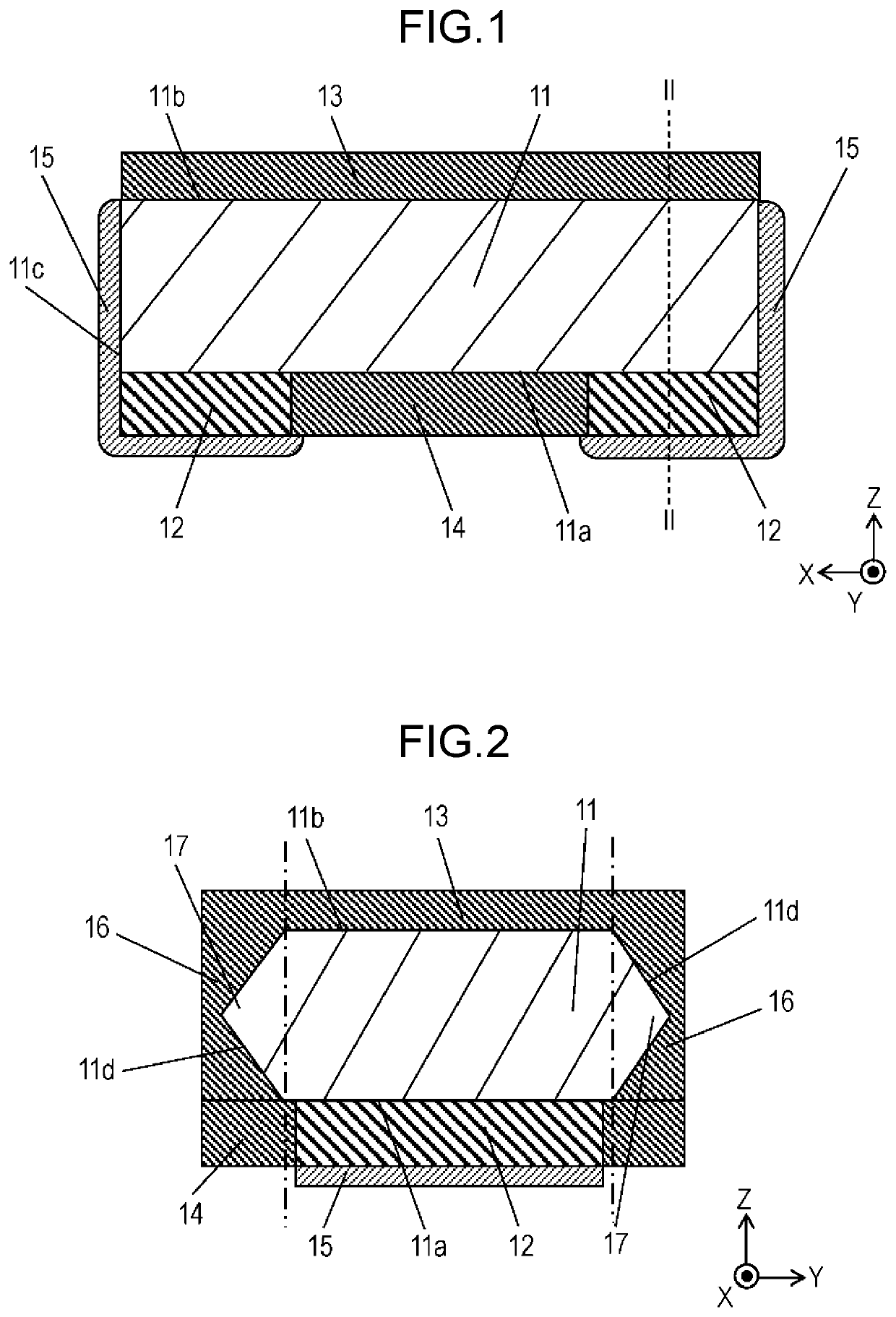
[0040]An exemplary embodiment of a chip resistor and a method for producing the chip resistor according to the present disclosure will be described below with reference to the drawings.

(1) Chip Resistor

[0041]FIG. 1 is a side view of the chip resistor according to the exemplary embodiment of the present disclosure. FIG. 2 is a cross-sectional view taken along line II-II in FIG. 1.

[0042]The chip resistor according to the exemplary embodiment of the present disclosure includes resistance member 11, electrodes 12, first protective film 13, second protective film 14, plated layer 15, and third protective film 16, as illustrated in FIG. 1 and FIG. 2. Resistance member 11 is formed of an alloy, for example, CuMnNi. Resistance member 11 includes first main surface 11a, second main surface 11b that is a rear surface of resistance member 11 when viewed from first main surface 11a, end surfaces 11c, and side surfaces 11d, end surfaces 11c and side surfaces 11d being located on respective later...


PUM


Abstract

An object of the present disclosure is to provide a chip resistor capable of suppressing degradation of long-term reliability, and a method for producing the chip resistor. The chip resistor of the present disclosure includes resistance member (11) formed of metal, and a pair of electrodes (12) respectively formed on both ends of first main surface (11a) of resistance member (11). The chip resistor further includes first protective film (13) formed on second main surface (11b) located on a rear side of first main surface (11a) of resistance member (11), second protective film (14) formed on first main surface (11a) of resistance member (11) and between the pair of electrodes (12), and a third protective film formed on a side surface parallel to a direction of a current flowing between the pair of electrodes (12) of resistance member (11). The side surface of resistance member (11) is provided with a protrusion that protrudes outward when viewed along the current flowing direction.

Description

TECHNICAL FIELD[0001]The present disclosure relates to a chip resistor that is used in various electronic devices and that uses a metal plate as a resistance member, and a method for producing the chip resistor.BACKGROUND ART[0002]As illustrated in FIGS. 8 and 9, a conventional chip resistor of this type includes resistance member 1 formed of metal, a pair of electrodes 2 respectively formed on both ends of first surface la of resistance member 1, first protective film 3 formed on second surface 1b opposite to first surface 1a of resistance member 1, second protective film 4 formed on first surface 1a of resistance member 1 and between the pair of electrodes 2, and plated layers 5 respectively formed from exposed surfaces of the pair of electrodes 2 to end surfaces of resistance member 1. In addition, third protective films 6 are respectively provided on side surfaces 1c of resistance member 1.[0003]A method for producing this chip resistor includes forming first protective film 3 o...

Claims


Application Information

Patent Timeline
IPC IPC(8): H01C1/14H01C7/00H01C17/00H01C1/01
CPCH01C7/00H01C1/14H01C1/01H01C17/006H01C1/034H01C1/02H01C7/001
Inventor KINOSHITA, YASUHARUTAMURA, TAKAAKI
Owner PANASONIC INTELLECTUAL PROPERTY MANAGEMENT CO LTD
Why Eureka
Try Eureka