
Display device

a display device and photo sensor technology, applied in the field of display devices, can solve the problems of sharp increase of parasitic capacitance, noise, and the ratio of the sensor node and the lead-out line, and achieve the effect of maximally secureing a storage capacity, minimizing the influence of noise, and minimizing the decrease of aperture ratio

Active Publication Date: 2020-02-27
LG DISPLAY CO LTD
View PDF0 Cites 1 Cited by
  • Summary
  • Abstract
  • Description
  • Claims
  • Application Information

AI Technical Summary

Benefits of technology

The present patent provides a display device that can minimize the impact of noise in a photo sensor type display device. It solves the problem of reduced aperture ratio and maximizes storage capacity, minimizing data signal changes. The device also overcomes issues caused by parasitic capacitors and simplifies touch circuit structures, reducing costs. Increased inch and resolution are possible by minimizing noise, and the device can be used in the DRD structure to maintain transmittance. Common lines can be added to minimize noise and reduce the number of lead-out lines by 50%. Overall, the device improves display performance and reduces noise impact in a photo sensor type display device.

Problems solved by technology

To this end, when the display and the sensing drive are divided by time division, the sensor node in the display panel needs to be read at one time due to the time division, there is disadvantage that one sensor node and one lead-out line must be matched at a ratio of 1:1.
On the other hand, since a photo sensor method in which the sensing and the display timing are simultaneously performed requires sensing at the time of driving the display, the ripple of a common voltage due to the display signal, that is, the transition of the data signal is transmitted to the lead-out line and thus noise occurs.
That is, the intensity of the noise is proportional to a parasitic capacitance applied to the lead-out line, but the parasitic capacitance increases sharply with increasing inches and resolution, and thus there is a problem in sensing.
However, the sensor storage capacitor has a side effect that affects an aperture ratio of the display panel.

Method used


Image

  • Display device
  • Display device
  • Display device

Examples


Embodiment Construction

[0034]Advantages and characteristics of the present disclosure and a method of achieving the advantages and characteristics will be clear by referring to exemplary aspects described below in detail together with the accompanying drawings. However, the present disclosure is not limited to the exemplary aspects disclosed herein but will be implemented in various forms. The exemplary aspects are provided by way of example only so that those skilled in the art can fully understand the disclosures of the present disclosure and the scope of the present disclosure. Therefore, the present disclosure will be defined only by the scope of the appended claims.

[0035]The shapes, sizes, ratios, angles, numbers, and the like illustrated in the accompanying drawings for describing the exemplary aspects of the present disclosure are merely examples, and the present disclosure is not limited thereto. Like reference numerals generally denote like elements throughout the specification. Further, in the f...


PUM

PropertyMeasurementUnit
sizeaaaaaaaaaa
critical dimensionaaaaaaaaaa
dimensionaaaaaaaaaa

Abstract

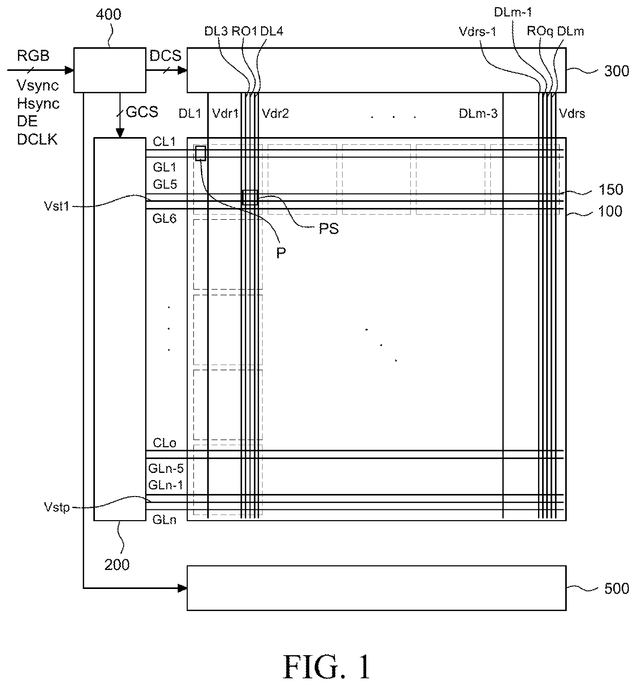
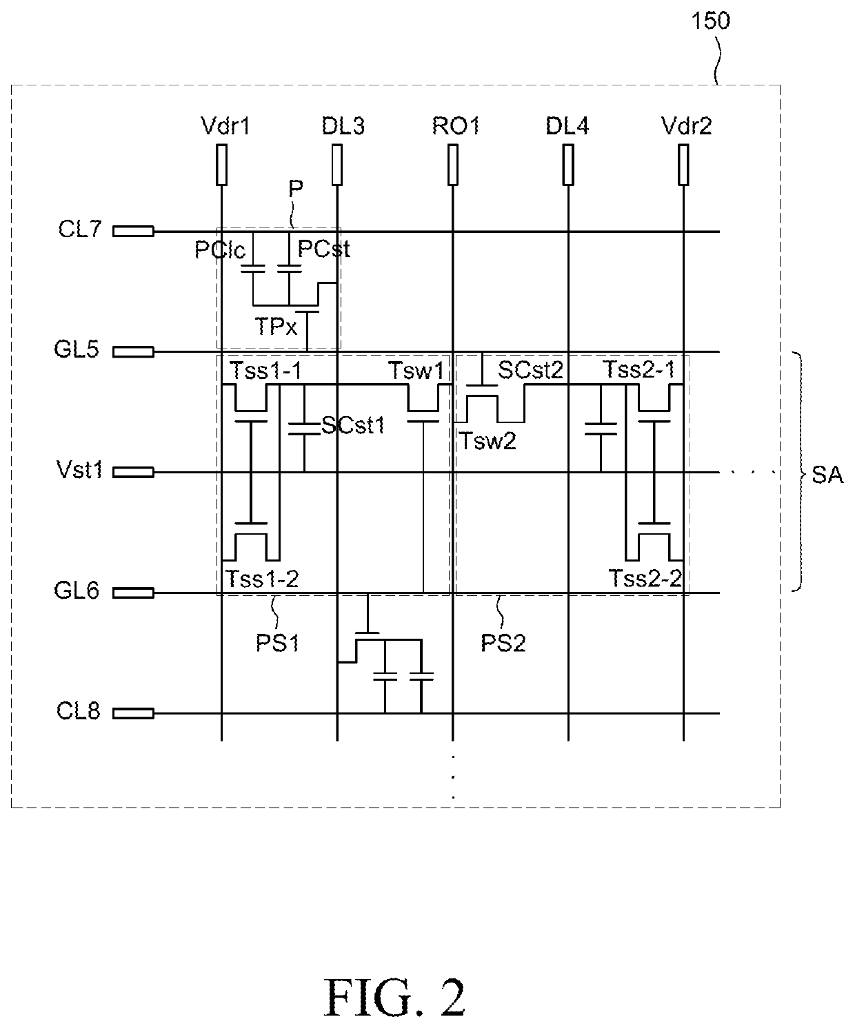
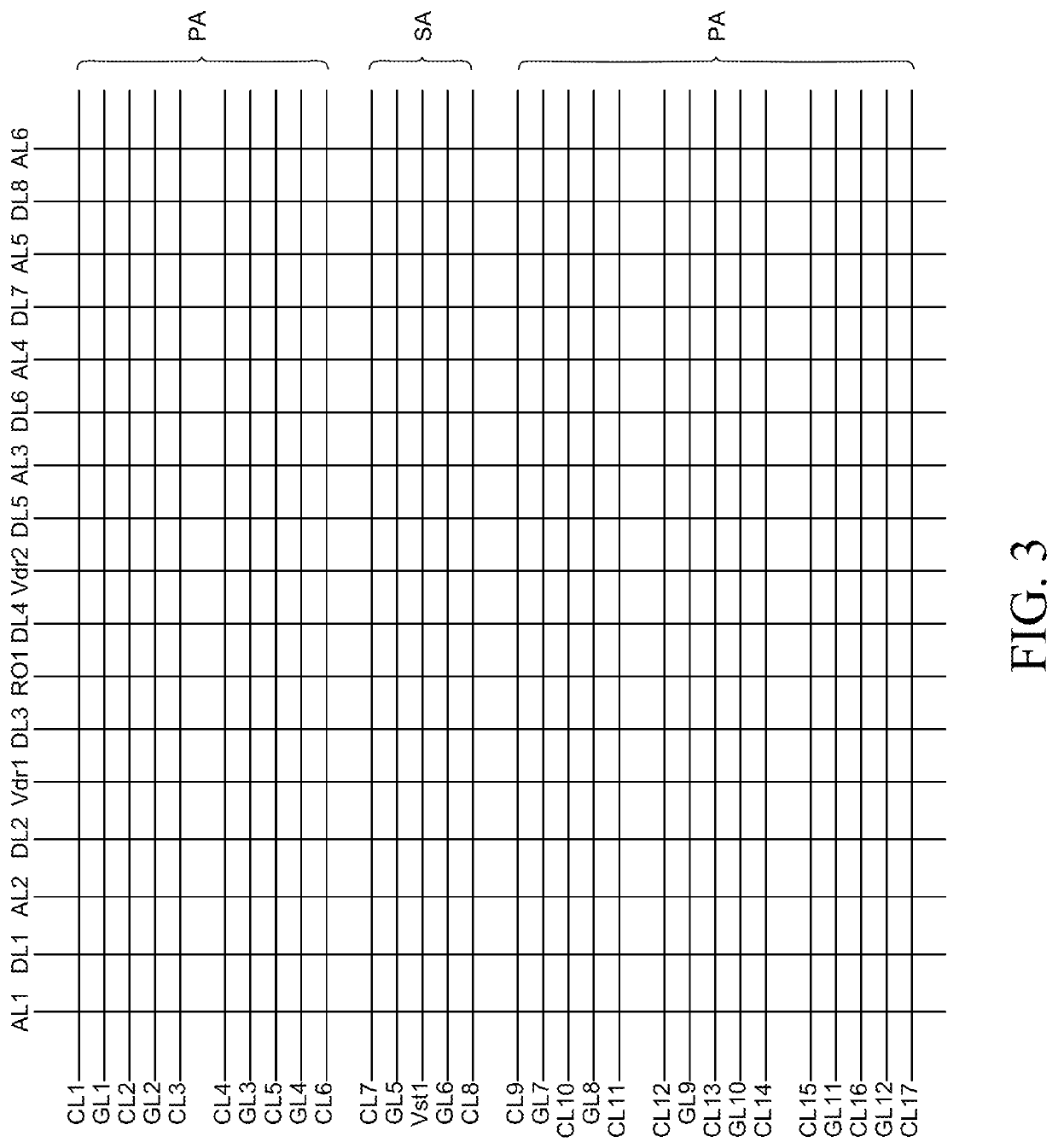
A display device according to an aspect of the present disclosure includes a lead-out line disposed between the data lines in the second direction, first and second photo touch sensors disposed in left and right pixels of the lead-out line and electrically connected to the lead-out line to transmit a touch sensing signal, first and second sensing data lines disposed in the second direction and applying first and second sensor data signals to the first and second photo touch sensors and first and second sensing gate lines disposed in the first direction and applying first and second sensor gate signals to the first and second photo touch sensors.

Description

CROSS-REFERENCE TO RELATED APPLICATION[0001]This application claims the priority of Korean Patent Application No. 10-2018-0097959 filed on Aug. 22, 2018, which is hereby incorporated by reference in its entirety.BACKGROUNDField of the Disclosure[0002]The present disclosure relates to a display device, and more particularly, to a photo sensor type display device.Description of the Background[0003]In the information age, a display field for visually expressing electrical information signals has been rapidly developed, and accordingly, various display devices having excellent performance such as thinning, light weight, and low power consumption have been developed.[0004]Examples of such a display device may include a liquid crystal display device (LCD), an organic light emitting display device (OLED), and the like.[0005]Recently, the display device has a touch screen that allows a user to easily input information or commands intuitively and conveniently by deviating from a conventional...

Claims


Application Information

Patent Timeline
Patent Type & Authority Applications(United States)
IPC IPC(8): G06F3/042G02F1/1333
CPCG06F3/0421G02F1/13338G06F3/0428G06F3/042G06F3/0416G02F1/136286G02F1/1343G02F1/1362G02F1/1335G02F1/13312
Inventor SHIN, SEUNGHWANSEO, DAEYOUNG
Owner LG DISPLAY CO LTD
Learn More