Stacked capacitor assembly structure
- Summary
- Abstract
- Description
- Claims
- Application Information
AI Technical Summary
Benefits of technology
Problems solved by technology
Method used
Image

Examples
first embodiment
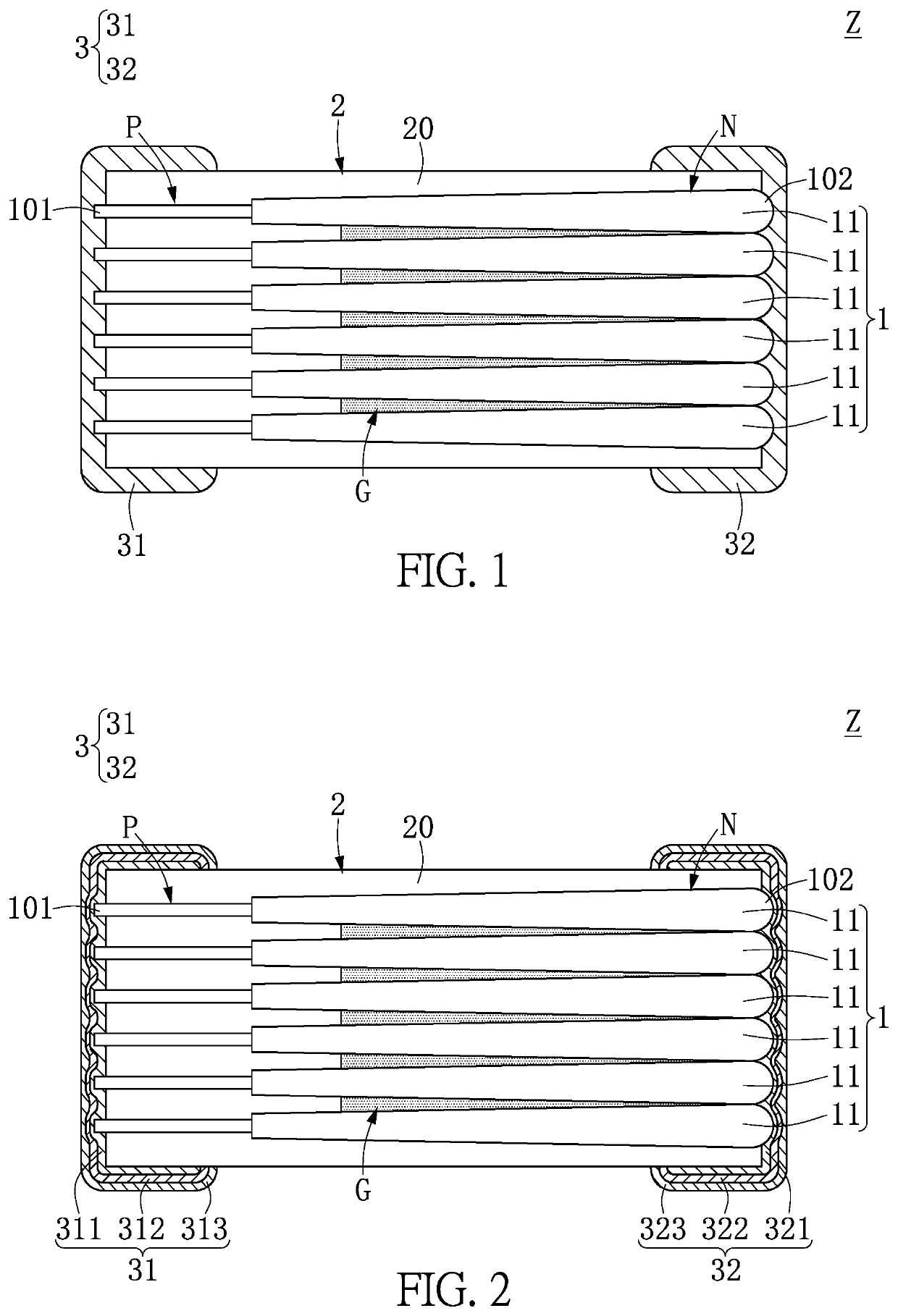
[0023]Referring to FIG. 1, a first embodiment of the present disclosure provides a stacked capacitor assembly structure Z including a capacitor unit 1, a package unit 2, and an electrode unit 3. For example, the stacked capacitor assembly structure Z may be a stacked capacitor package structure, a stacked capacitor component belonging to a component type, or a stacked solid electrolytic capacitor defined by the type of use.
[0024]First, the capacitor unit 1 includes a plurality of stacked capacitors 11, and each of the stacked capacitors 11 has a positive portion P and a negative portion N. Further, a plurality of stacked capacitors 11 are sequentially stacked, and each of the two stacked capacitors 11 can be electrically connected to each other through a conductive adhesive Cc and the plurality of positive electrode portions P of the plurality of stacked capacitors 11 are separated from each other without contact. For example, the stacked capacitor 11 includes a metal foil, an oxide...
second embodiment
[0029]Referring to FIG. 2, a second embodiment of the present disclosure provides a stacked capacitor assembly structure Z including a capacitor unit 1, a package unit 2, and an electrode unit 3, the main difference between the first embodiment and the second embodiment of the present disclosure is that, as can be seen from a comparison between FIG. 2 and FIG. 1, in the second embodiment, the first electrode structure 31 includes a first inner conductive layer 311 covering the first exposed portion 101 and electrically contacting the positive electrode portion P, and a first intermediate conductive layer covering the first inner conductive layer 311. The layer 312 and a first outer conductive layer 313 covering the first intermediate conductive layer 312. In addition, the second electrode structure 32 includes a second inner conductive layer 321 covering the second exposed portion 102 and electrically contacting the negative portion N, a second intermediate conductive layer 322 cove...
third embodiment
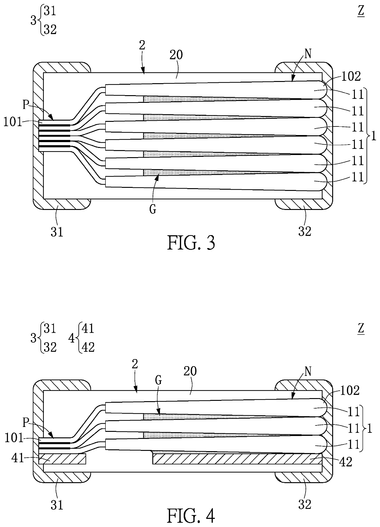
[0031]Referring to FIG. 3, a third embodiment of the present disclosure provides a stacked capacitor assembly structure Z including a capacitor unit 1, a package unit 2, and an electrode unit 3, the main difference between the first embodiment and the third embodiment of the present disclosure is that, as can be seen from a comparison between FIG. 3 and FIG. 1 in the third embodiment, the plurality of positive portions P of the plurality of stacked capacitors 11 are sequentially stacked. For example, the plurality of positive portions P may be sequentially stacked by laser welding, impedance welding, or other kinds of welding methods, however, the present disclosure is not limited thereto.
[0032]It should be noted that the first electrode structure 31 and the second electrode structure 32 of the electrode unit 3 of the third embodiment can be replaced with the first electrode structure 31 and the second electrode structure 32 of the electrode unit 3 disclosed in the second embodiment...
PUM
 Abstract
Description
Claims
Application Information
 - R&D Engineer
- R&D Manager
- IP Professional
- Industry Leading Data Capabilities
- Powerful AI technology
- Patent DNA Extraction
Browse by: Latest US Patents, China's latest patents, Technical Efficacy Thesaurus, Application Domain, Technology Topic.
© 2024 PatSnap. All rights reserved.Legal|Privacy policy|Modern Slavery Act Transparency Statement|Sitemap