Avalanche diode based object detection device

an object detection and diode technology, applied in the field of optical object detection devices, can solve the problems of affecting detection results, affecting detection accuracy,

Active Publication Date: 2020-03-19
PIXART IMAGING INC
View PDF0 Cites 4 Cited by
  • Summary
  • Abstract
  • Description
  • Claims
  • Application Information

AI Technical Summary

Benefits of technology

[0015]In the object detection device of the present disclosure, energy of ambient light is also indicated by event counts. The influence of ambient light

Problems solved by technology

However, an operation environment of a distance detection device generally exists both light source signals and ambient light, and thus in addition to avalanche events triggered by the light source signals, avalanche ev

Method used


Image

  • Avalanche diode based object detection device
  • Avalanche diode based object detection device
  • Avalanche diode based object detection device

Examples


first embodiment

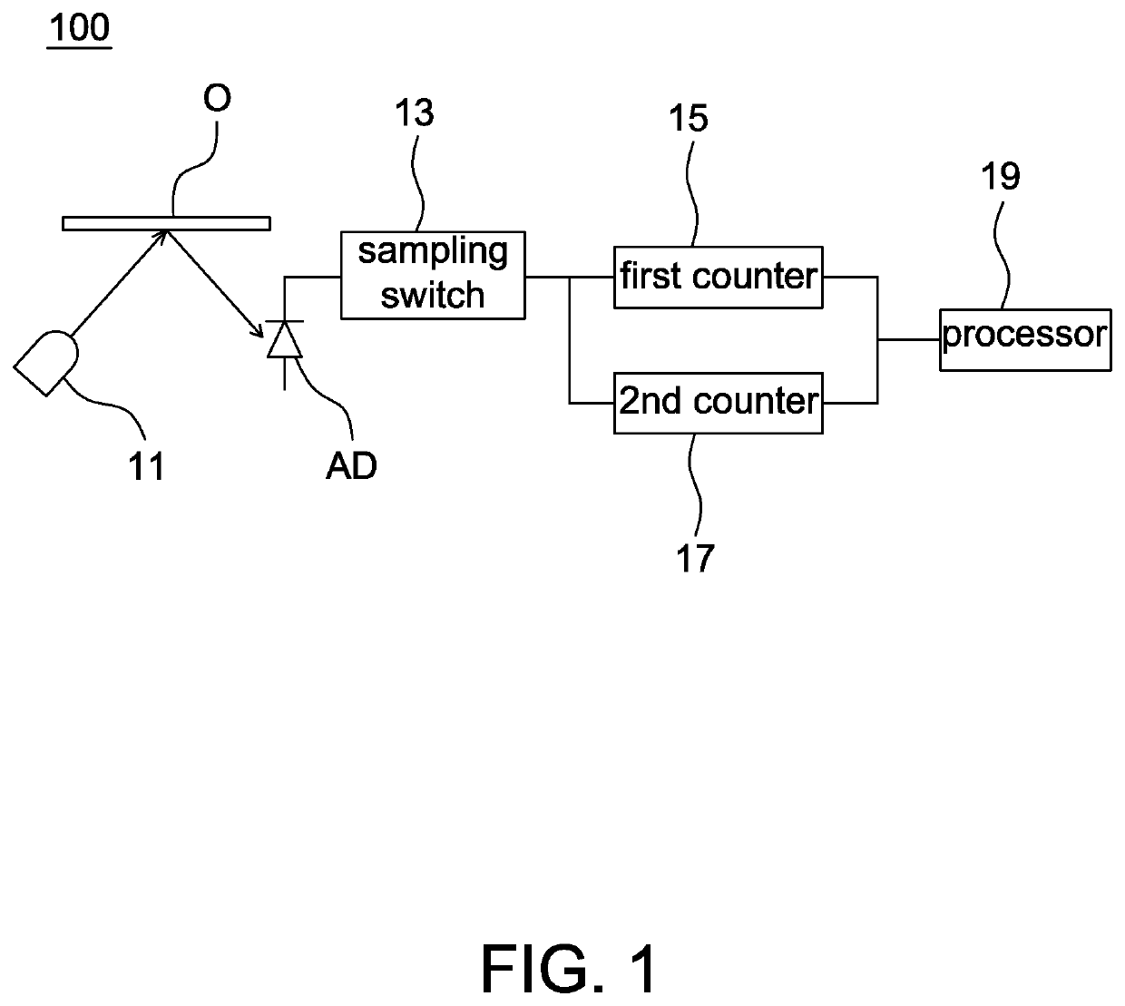
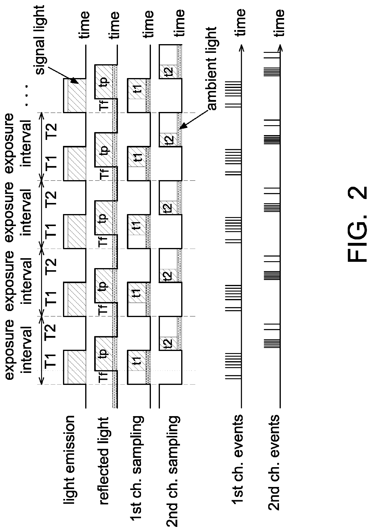
[0027]Referring to FIG. 2, one example of the object detection device 100 according to the present disclosure is illustrated hereinafter.

[0028]The light source 11 is a laser diode (LD), e.g., VCSEL. The light source 11 emits light toward an object O with an identifiable spectrum (e.g., red light and / or infrared light), wherein the object O is any object within a detectable distance of the object detection device 100 without particular limitations as long as the object O reflects the light emitted by the light source 11. For example, FIG. 2 shows that the light source 11 is turned on to emit light within a first interval T1 and turned off within a second interval T2, and the light source 11 operates repeatedly in this way. For example, one exposure interval=T1+T2.

[0029]FIG. 2 shows that after the light source 11 is turned on to emit light, the emitted light reaches the avalanche diode AD after being reflected by the object O by a time interval Tf. The avalanche diode AD is, for examp...

second embodiment

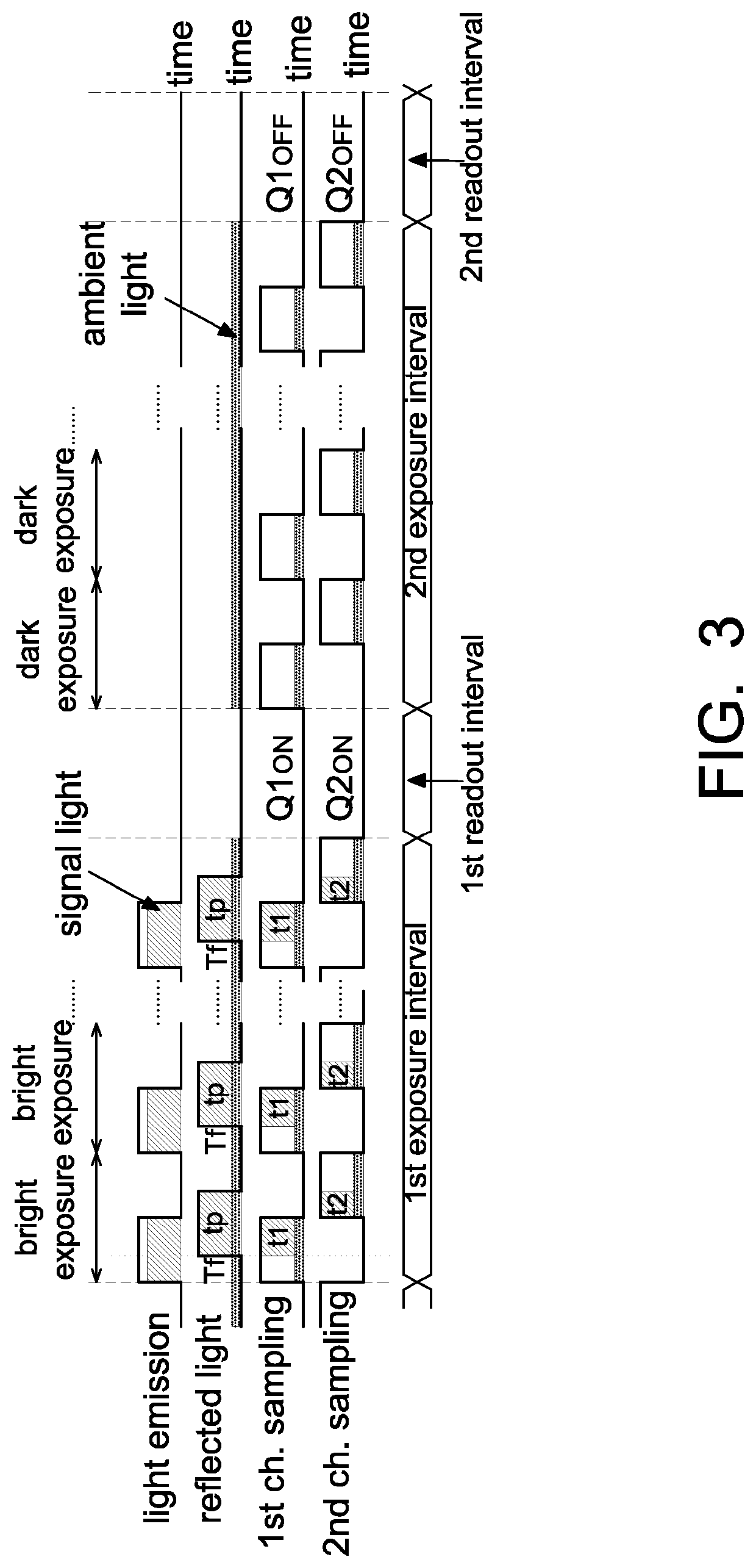
[0039]To reduce the influence from ambient light, the differential operation between bright exposures and dark exposures is performed. For example referring to FIG. 3, it is an operational schematic diagram of an object detection device according to the present disclosure, which is also adaptable to the object detection device 100 in FIG. 1.

[0040]In the embodiment of FIG. 3, a first exposure interval includes a plurality of bright exposures, and the operation of each bright interval is identical to that of one exposure interval (T1+T2) in FIG. 2, and thus FIG. 3 omits the timing diagram of events. Accordingly, in the first exposure interval, the first counter 15 accumulates a first count value Q1ON which is N times of avalanche events of the first channel in one exposure interval of FIG. 2, e.g., Q1ON=N×CN1 (referring to equation 1). Similarly, the second counter 17 accumulates a second count value Q2ON which is N times of avalanche events of the second channel in one exposure inter...

third embodiment

[0046]Referring to FIG. 4, it is an operational schematic diagram of an object detection device according to the present disclosure, which is also implemented by the object detection device 100 of FIG. 1. The difference between FIG. 3 and FIG. 4 is that in FIG. 4, bright exposures and dark exposures are arranged adjacent to each other to further reduce the influence of time-changed ambient light.

[0047]As shown in FIG. 4, the light source 11 is turned on to emit light toward the object O within a first interval T1, and is turned off in a second interval T2, a third interval T3 and a fourth interval T4. In this embodiment, the first interval T1, the second interval T2, the third interval T3 and the fourth interval T4 form one exposure interval, e.g., one exposure interval=T1+T2+T3+T4, and T1 to T4 are preferably the same. As the first sampling channel detects the energy of light source signal in the first time interval T1, and the second sampling channel detects the energy of light so...


PUM


Abstract

There is provided an object detection device including a light source, an avalanche diode, a first counter, a second counter and a processor. The light source emits light within a first interval, and is turned off within a second interval, a third interval and a fourth interval. The avalanche diode detects photons corresponding to the first interval, second, third and fourth intervals to trigger avalanche events. The first counter performs up-counting on the avalanche events in the first interval and performs down-counting on the avalanche events in the third interval to generate a first count value. The second counter performs up-counting on the avalanche events in the second interval and performs down-counting on the avalanche events in the fourth interval to generate a second count value. The processor calculates a time-of-flight according to the first count value and the second count value.

Description

BACKGROUND1. Field of the Disclosure[0001]This disclosure generally relates to an optical object detection device and, more particularly, to an object detection device for calculating a time-of-flight according to a count value for counting avalanche events of an avalanche diode.2. Description of the Related Art[0002]Nowadays, the optical distance detection device generally adopts the imaging technique based on a CCD image sensor or a CMOS image sensor. The method of calculating an object distance according to a shifted time from a light beam emitted from a light source, reflected by an object and finally received by an image sensor is referred to the time-of-flight technique.[0003]In processing light signals in a weak light environment and having a high frequency, the single photon detection is another choice.[0004]For example, a single photon avalanche diode (SPAD) is used as an indicator of reflected light. When a photon is received by the SPAD, an avalanche current is triggered ...

Claims


Application Information

Patent Timeline
IPC IPC(8): G01S7/487G01S17/02G01S7/486
CPCG01S17/04G01S7/487G01S7/4865G01S7/4861G01S17/10G01S17/36G01S7/493G01S7/4915G01S17/894G01S7/4914
Inventor TSAI, TSO-SHENG
Owner PIXART IMAGING INC
Why Eureka
Try Eureka