

Display panel and display
a display panel and display panel technology, applied in static indicating devices, instruments, non-linear optics, etc., can solve problems such as signal transmission delay, and achieve the effects of reducing the area of intersection, reducing capacitance, and reducing the signal delay time of the display panel
- Summary
- Abstract
- Description
- Claims
- Application Information
AI Technical Summary
Benefits of technology
Problems solved by technology
Method used
Image

Examples
Embodiment Construction
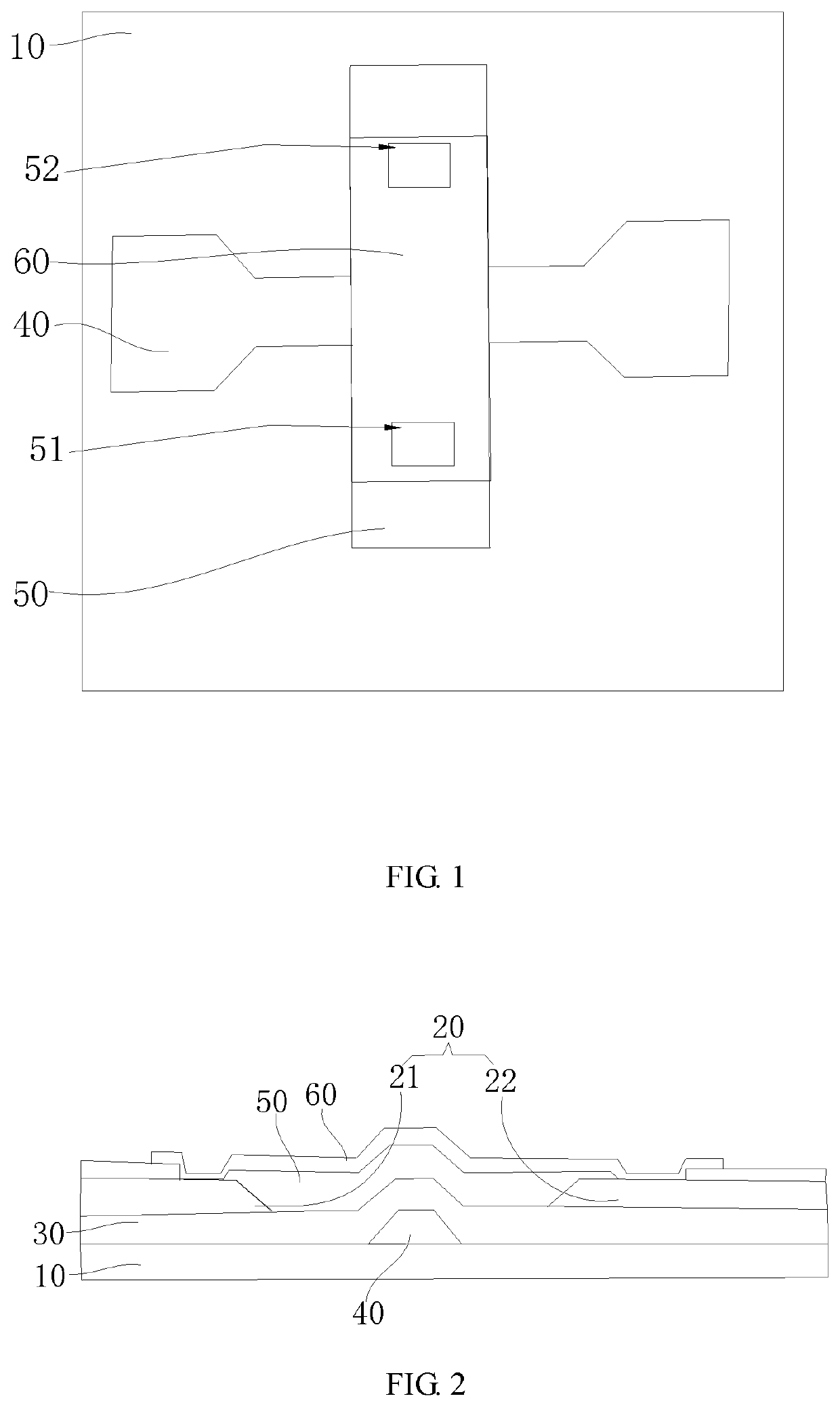
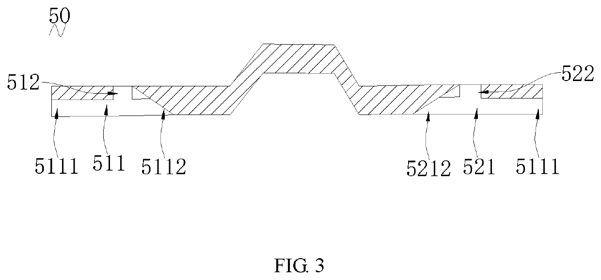
[0051]The technical solutions in the embodiments of the present disclosure will be clearly described in the following with reference to the accompanying drawings in the embodiments of the present disclosure. It is obvious that the embodiments to be described are just some instead of all embodiments of the present disclosure. All other embodiments obtained by those skilled in the art based on the embodiments of the present disclosure without paying any creative effort should be included within the protection scope of the present disclosure.
[0052]The term “comprise” and its variations in the specification, claims and above description of the drawings of the present disclosure are intended to cover non-exclusive inclusions. For example, a process, method or system, product or device including a series of steps or units is not limited to the listed steps or units, but optionally also includes steps or units not listed, or optionally also includes other steps or units inherent to the pro...
PUM
| Property | Measurement | Unit |
|---|---|---|
| conductive | aaaaa | aaaaa |
| size | aaaaa | aaaaa |
| circumference | aaaaa | aaaaa |
Abstract
Description
Claims
Application Information