Electronic component module, and manufacturing method for electronic component module

a manufacturing method and electronic component technology, applied in the direction of circuit electrical arrangement, cross-talk/noise/interference reduction, basic electric elements, etc., can solve the problems of high possibility, degraded characteristics, and susceptible to electromagnetic waves from the outside of the electronic component or the wiring layer, so as to reduce the degradation of electromagnetic shielding performance to block electromagnetic waves from the outside, the effect of preventing or reducing the degradation

Active Publication Date: 2020-05-28
MURATA MFG CO LTD
View PDF0 Cites 0 Cited by
  • Summary
  • Abstract
  • Description
  • Claims
  • Application Information

AI Technical Summary

Benefits of technology

[0011]With the electronic component modules and the manufacturing methods for electronic component modules according to preferred embodiments of t

Problems solved by technology

However, with an existing electronic component module as in the case of the semiconductor package described in Japanese Unexamined Patent Application Publication No. 2005-310954, there is a problem in that, for example, the electronic component or the wiring layers are susceptible to electromagnetic waves from the outside.
Thus, with the existing electronic component module described in Japanese Unexamined Patent Ap

Method used


Image

  • Electronic component module, and manufacturing method for electronic component module
  • Electronic component module, and manufacturing method for electronic component module
  • Electronic component module, and manufacturing method for electronic component module

Examples


first preferred embodiment

(1) General Configuration of Electronic Component Module

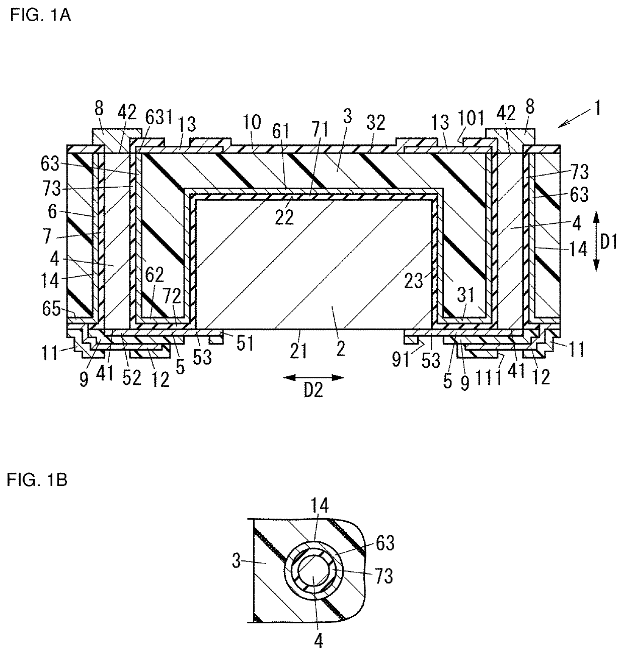
[0027]Hereinafter, an electronic component module 1 according to a first preferred embodiment of the present invention will be described with reference to the drawings.

[0028]As shown in FIG. 1A, the electronic component module according to the first preferred embodiment includes an electronic component 2, a resin structure 3, a plurality of (two in the illustrated example) through-wires 4, a plurality of (two in the illustrated example) wiring layers (wiring portions) 5, an electrically conductive shield portion 6, and an electrically insulating portion (intermediate portion) 7 having an electrically insulating property. In the electronic component module 1, the resin structure 3 holds the electronic component 2 and the through-wires 4. In the electronic component module 1, the resin structure 3 protects the electronic component 2 against impact, or the like, from the outside. The through-wires 4 are located to the sides of the...

first modification

(5.1) First Modification

[0086]As shown in FIG. 6, an electronic component module 1a according to a first modification of the first preferred embodiment differs from the electronic component module 1 according to the first preferred embodiment in that the first grounding wiring layers 12 and the third resist layers 11 in the electronic component module 1 (see FIG. 1A) according to the first preferred embodiment are not provided. As for the electronic component module 1a according to the first modification, the same reference numerals denote the same or similar elements to those of the electronic component module 1 according to the first preferred embodiment, and the description thereof is omitted.

[0087]In the electronic component module 1a according to the first modification, the first grounding wiring layers 12 and the third resist layers 11 are not provided, so manufacturing is facilitated as compared to the electronic component module 1 of the first preferred embodiment.

second modification

(5.2) Second Modification

[0088]As shown in FIG. 7, an electronic component module 1b according to a second modification of the first preferred embodiment differs from the electronic component module 1 according to the first preferred embodiment in that the first resist layers 9 each cover the entire or substantially the entire wiring layer 5 and the first grounding wiring layers 12 each cover the entire or substantially the entire first resist layer 9. As for the electronic component module 1b according to the first modification, the same reference numerals denote the same or similar elements to those of the electronic component module according to the first preferred embodiment, and the description thereof is omitted.

[0089]With the electronic component module 1b according to the second modification, radio-frequency signals that pass through the wiring layers 5 are insusceptible to electromagnetic waves from the outside of the electronic component module 1. Thus, with the electronic...


PUM


Abstract

An electronic component module includes an electronic component, a resin structure, a wiring portion, and a shield portion. The resin structure covers a second main surface and at least a portion of a side surface of the electronic component. The wiring portion is electrically connected to the electronic component. The shield portion includes a first conductor layer and a second conductor layer. The first conductor layer is spaced away from the electronic component between the electronic component and the resin structure, and has electrical conductivity. The second conductor layer is spaced away from the wiring portion between the wiring portion and the resin structure, and has electrical conductivity. In the shield portion, the first conductor layer and the second conductor layer are integrated.

Description

CROSS REFERENCE TO RELATED APPLICATIONS[0001]This application claims the benefit of priority to Japanese Patent Application No. 2017-158855 filed on Aug. 21, 2017 and is a Continuation Application of PCT Application No. PCT / JP2018 / 030183 filed on Aug. 13, 2018. The entire contents of each application are hereby incorporated herein by reference.BACKGROUND OF THE INVENTION1. Field of the Invention[0002]The present invention relates to an electronic component module, and a manufacturing method for an electronic component module and, more specifically, to an electronic component module including an electronic component and a resin structure, and a manufacturing method for an electronic component module.2. Description of the Related Art[0003]Hitherto, a semiconductor package including a semiconductor chip (electronic component), an electrically insulating resin layer (resin structure), electrically conductive posts (through-wires), connection terminals, wiring layers, and a surface layer...

Claims


Application Information

Patent Timeline
IPC IPC(8): H01L23/31H01L23/00H01L23/552H01L25/11H01L21/56H05K1/02H01L23/13
CPCH01L24/97H05K1/0216H01L23/13H01L23/3121H01L2224/04105H01L24/96H01L2924/3025H01L21/565H01L23/552H01L21/568H01L25/117H01L24/04H01L2224/0401H01L23/5389H01L23/49811H01L23/49816H01L21/6835H01L23/3185H01L23/3128H01L2221/68345H01L2221/68327H01L2221/68381H01L24/20H01L2224/18H01L2224/16237H01L2224/16238H01L2224/16235H01L2224/1703H01L2224/131H01L2224/13144H01L2224/81192H03H9/0547H03H9/0557H03H9/059H03H9/1071H03H9/1078H03H9/02992H03H3/08H01L23/3135H01L25/16H01L2924/0001H01L2924/014H01L2924/00014
Inventor IWAMOTO, TAKASHI
Owner MURATA MFG CO LTD
Why Eureka
Try Eureka