Methods And Systems For Inspection Of Semiconductor Structures With Automatically Generated Defect Features

a technology of automatic generation and defect features, applied in the field of specimen inspection, can solve the problems of high aspect ratio structures that create challenges for patterned wafer inspection, no guarantee that the selected attribute or set of attributes optimally captures the desired separation, and no guarantee that the selected attribute or set of attributes optically classifies the dois, etc., and achieves the effect of reducing the number of attributes employed

Active Publication Date: 2020-07-23
KLA CORP
View PDF0 Cites 24 Cited by
  • Summary
  • Abstract
  • Description
  • Claims
  • Application Information

AI Technical Summary

Benefits of technology

[0014]The combination of deep learning and independent statistical classifiers to guide the reducing of a deep learning based model provides a direct performance-driven approach to minimize the computational cost of determining attributes without losing performance.
[0016]In another further aspect, the training of a statistical classifier is performed in an iterative manner while reducing the number of attributes employed in the training of the defect classifier.

Problems solved by technology

Such high aspect ratio structures create challenges for patterned wafer inspection.
There is no guarantee that the selected attribute or set of attributes optimally captures the desired separation between DOIs and nuisance defects.
Further, there is no guarantee that the selected attribute or set of attributes optically classifies the DOIs.
Thus, it is highly likely that a classification model trained based on manually selected attributes will underperform.
This becomes limiting as inspection applications become more and more challenging.
However, the computational cost of executing a complex, trained neural network for inline wafer inspection is excessively high.
Thus, high throughput at an acceptable cost has not been attained.
Furthermore, it has not been possible to integrate human knowledge of defect classification or information beyond the available optical images to enhance the training process.
Thus, currently, a classification model trained based on a neural network to operate directly on images cannot benefit from human knowledge or additional signal information that might further improve performance of the trained classifier.

Method used


Image

  • Methods And Systems For Inspection Of Semiconductor Structures With Automatically Generated Defect Features
  • Methods And Systems For Inspection Of Semiconductor Structures With Automatically Generated Defect Features
  • Methods And Systems For Inspection Of Semiconductor Structures With Automatically Generated Defect Features

Examples


Embodiment Construction

[0029]Reference will now be made in detail to background examples and some embodiments of the invention, examples of which are illustrated in the accompanying drawings.

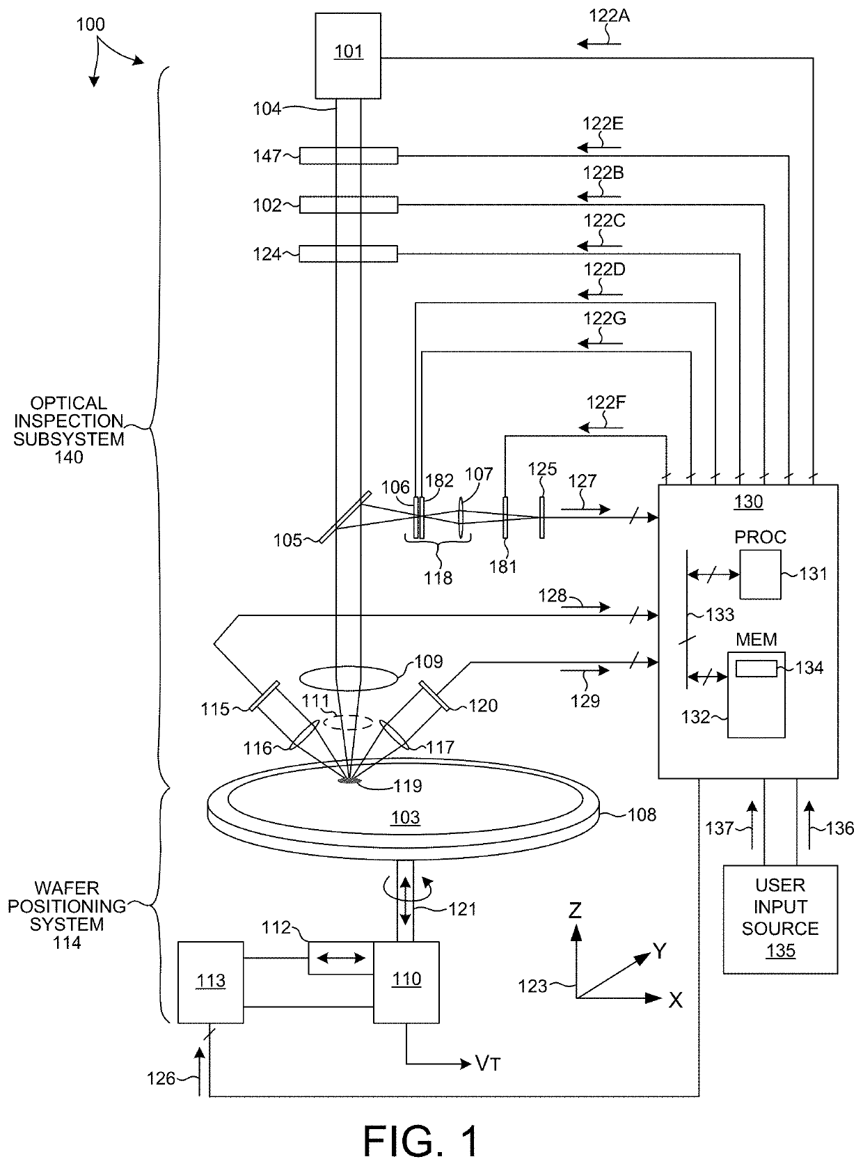
[0030]Methods and systems for improved detection and classification of defects of interest (DOI) within semiconductor structures are described herein. In particular, nuisance filtering and defect classification based on optical inspection is realized by estimating the values of one or more automatically generated attributes derived from images of a candidate defect. A statistical classifier is trained to classify defects based on the values of the automatically generated attributes.

[0031]The automatically generated attributes are determined by iteratively training, reducing, and retraining a deep learning model. The deep learning model relates optical images of candidate defects to a known classification of those defects. The deep learning model is iteratively reduced in complexity, while maintaining sufficient classi...


PUM


Abstract

Methods and systems for improved detection and classification of defects of interest (DOI) is realized based on values of one or more automatically generated attributes derived from images of a candidate defect. Automatically generated attributes are determined by iteratively training, reducing, and retraining a deep learning model. The deep learning model relates optical images of candidate defects to a known classification of those defects. After model reduction, attributes of the reduced model are identified which strongly relate the optical images of candidate defects to the known classification of the defects. The reduced model is subsequently employed to generate values of the identified attributes associated with images of candidate defects having unknown classification. In another aspect, a statistical classifier is employed to classify defects based on automatically generated attributes and attributes identified manually.

Description

CROSS REFERENCE TO RELATED APPLICATION[0001]The present application for patent claims priority under 35 U.S.C. § 119 from Patent Application No. 201941002244 at the Government of India Patent Office, filed Jan. 18, 2019, and claims priority under 35 U.S.C. § 119 from U.S. provisional patent application Ser. No. 62 / 896,578, filed Sep. 6, 2019. The subject matter of each prior filed application is incorporated herein by reference in its entirety.TECHNICAL FIELD[0002]The described embodiments relate to systems for specimen inspection, and more particularly to semiconductor wafer inspection.BACKGROUND INFORMATION[0003]Semiconductor devices such as logic and memory devices are typically fabricated by a sequence of processing steps applied to a substrate or wafer. The various features and multiple structural levels of the semiconductor devices are formed by these processing steps. For example, lithography among others is one semiconductor fabrication process that involves generating a pat...

Claims


Application Information

Patent Timeline
Patent Type & Authority Applications(United States)
IPC IPC(8): G06T7/00G06N3/08G06K9/62G06V10/764
CPCG06K9/6257G06T2207/30148G06T7/0004G06T2207/20081G06T2207/20224G06T2207/20084G06K9/6267G06N3/08G06N3/082G06N20/10G06N20/20G06V10/764G06N5/01G06N3/045G06F18/2413G06F18/2148G06F18/24H01L22/12H01L22/20
Inventor GEORGE, JACOBPARAMASIVAM, SARAVANANPLIHAL, MARTINNARASIMHAN, NIVEDITHA LAKSHMIRAVU, SAIRAMUPPALURI, PRASANTI
Owner KLA CORP
Why Eureka
Try Eureka