Thin film package structure and thin film package method of organic light emitting diode display

a light-emitting diode and thin film technology, applied in the field of display, can solve the problems of device failure, loss of water and oxygen resistance, failure of the package layer, etc., and achieve the effects of improving the brittleness of inorganic materials, enhancing the strength and tenacity of a matrix, and good thermal conductivity of metal nanoparticles

Inactive Publication Date: 2020-07-30
WUHAN CHINA STAR OPTOELECTRONICS SEMICON DISPLAY TECH CO LTD
View PDF0 Cites 2 Cited by
  • Summary
  • Abstract
  • Description
  • Claims
  • Application Information

AI Technical Summary

Benefits of technology

[0005]The present invention relates to a thin film package structure and a thin film package method of an organic light emitting diode display to solve the brittleness problems that stress concentration or even crack is easily generated in the inorganic layer of the thin film package structure.
[0025]Compared with the prior art, the inorganic layer of the thin film package structure of the organic light emitting diode display according to the present invention is doped with metal nanoparticles, which can prevent cracks propagation, effectively enhance the strength and tenacity of a matrix, and effectively achieve a purpose of improving brittleness of the inorganic materials in the thin film package structure. Also, a good thermal conductivity of the metal nanoparticles can effectively improve the heat dissipation performance of the organic light emitting diode display.

Problems solved by technology

At present, organic materials for an organic light emitting diode display (OLED) display are highly susceptible to water and oxygen in the air, resulting in device failure.
Inorganic materials are brittle by their nature, and cracks and even crack propagation are prone to occur during bending, resulting in failure of the package layer and loss of water and oxygen resistance.
In order to improve the bending property of the inorganic layer, it is generally required to form the inorganic layer into a special shape of a zigzag or a wave shape to relieve stress, but there is still a risk of tendency to create or even exacerbate local stress concentration at chamfers of these special shapes, which are more likely to cause cracks.
Therefore, in the conventional thin film package technology of an organic light emitting diode display, there are still brittleness problems that stress concentration or even crack is easily generated in the inorganic layer of the thin film package structure, and improvement is urgently required.

Method used


Image

  • Thin film package structure and thin film package method of organic light emitting diode display
  • Thin film package structure and thin film package method of organic light emitting diode display

Examples


Embodiment Construction

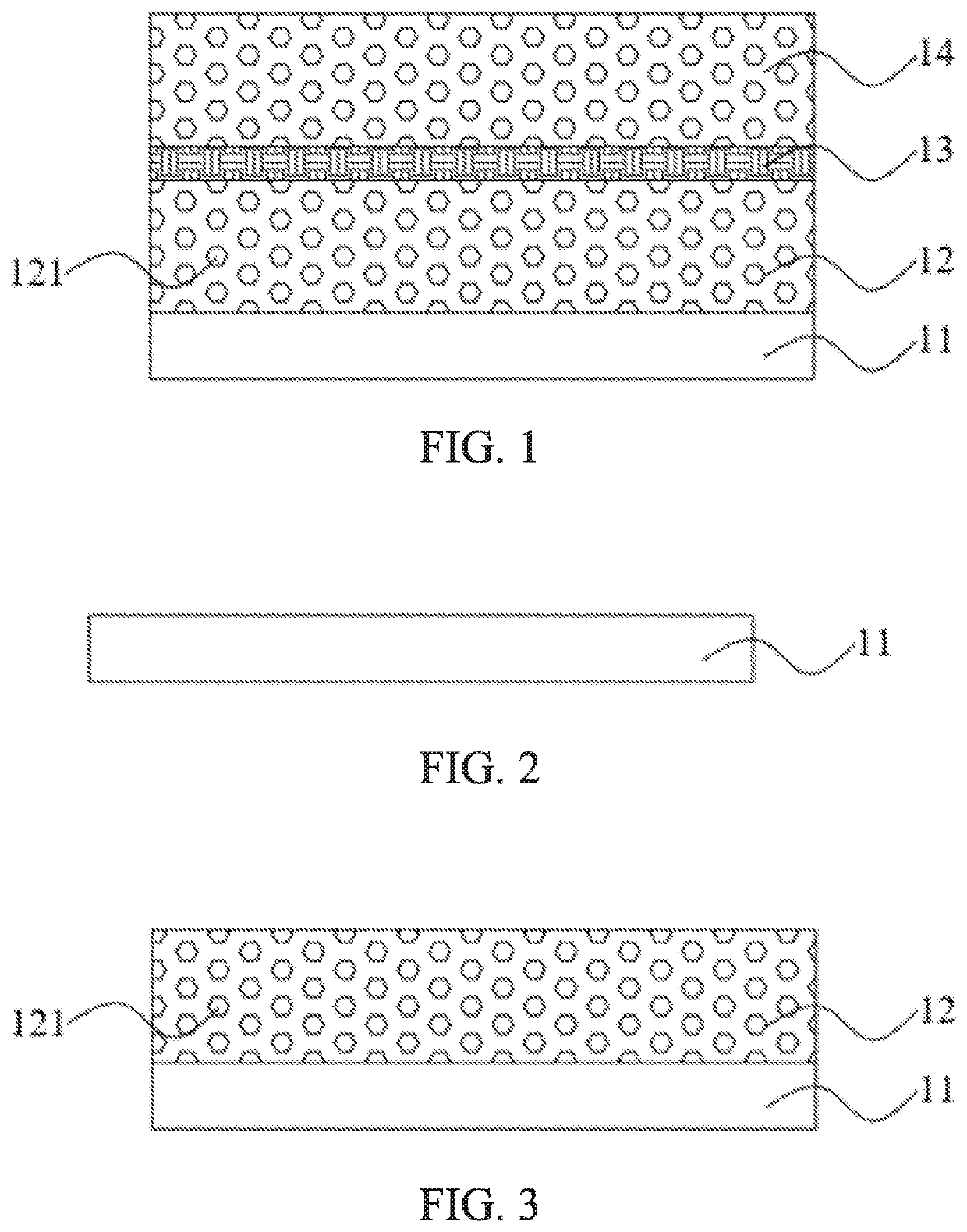
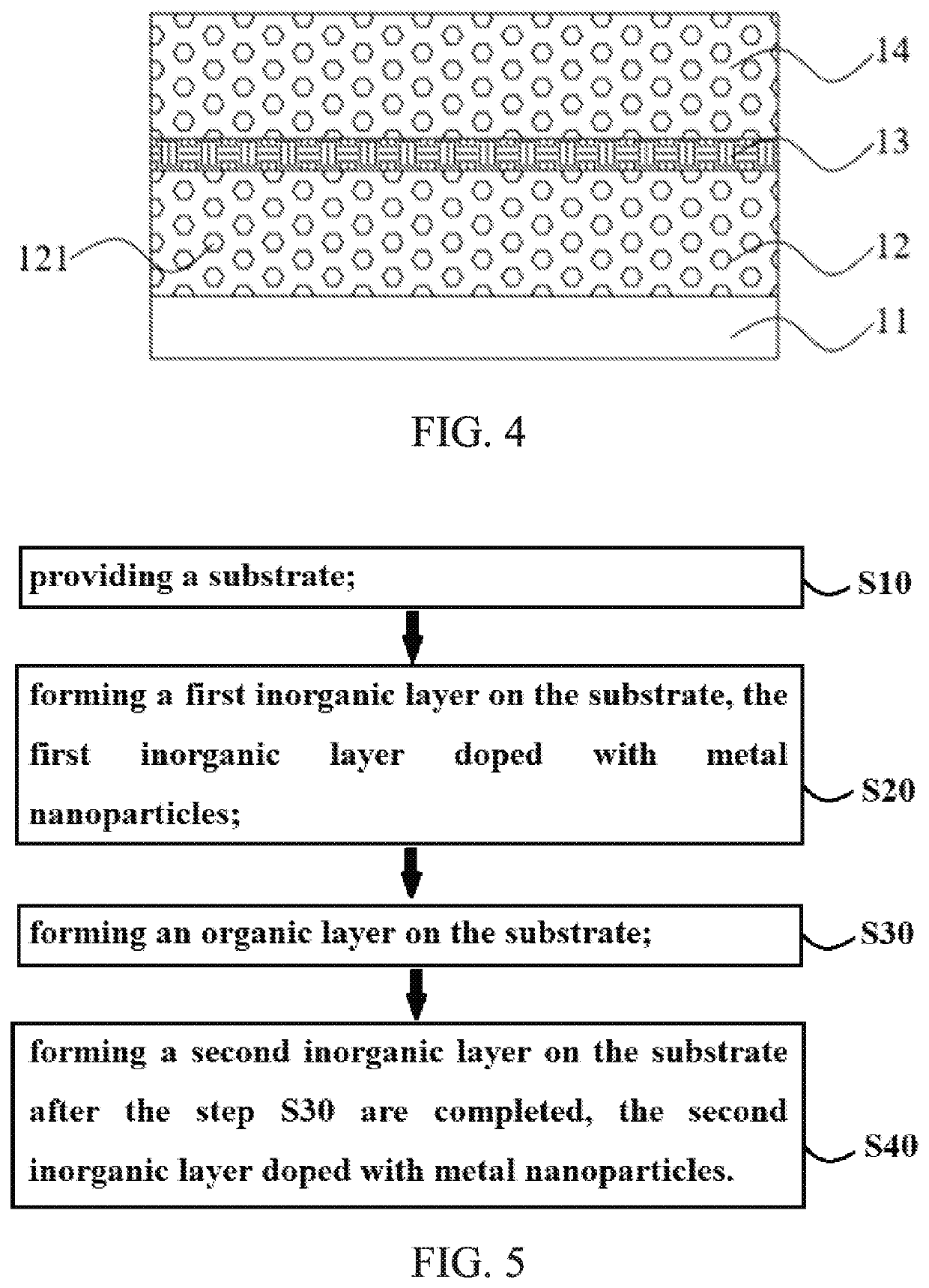
[0032]Please refer to the figures in the drawings, in which, like numbers refer to like elements throughout the description of the figures. Hereinafter, the present invention will be described in further detail with reference to examples. It is to be understood, however, that these examples are for illustrative purposes only and are not intended to limit the scope of the present invention.

[0033]In the description of the present invention, it is to be understood that the terms “center”, “lateral”, “upper”, “lower”, “left”, “right”, “vertical”, “horizontal”, “top”, “bottom”, “inside”, “outside” and the like are based on the orientation or positional relationship shown in the drawings, and is merely for the convenience of describing the present invention and simplifying the description, and does not indicate or imply that the indicated devices or components must to be in particular orientations, or constructed and operated in a particular orientation, and thus are not to be construed a...


PUM

PropertyMeasurementUnit
thicknessaaaaaaaaaa
thicknessaaaaaaaaaa
vol %aaaaaaaaaa

Abstract

The present invention provides a thin film package structure of an organic light emitting diode (OLED) display, comprising an inorganic layer and an organic layer, wherein the inorganic layer and the organic layer are formed on a substrate, and the inorganic layer and the organic layer are alternately disposed, wherein the inorganic layer comprises an inorganic polymer doped with metal nanoparticles.

Description

BACKGROUND OF INVENTIONField of Invention[0001]The present invention relates to a field of display, and in particular to a thin film package structure and a thin film package method of an organic light emitting diode display.Description of Prior Art[0002]At present, organic materials for an organic light emitting diode display (OLED) display are highly susceptible to water and oxygen in the air, resulting in device failure. Therefore, it is necessary to package the OLED device and require a water oxygen transmission rate of less than 10-6 g / m2d. A common conventional OLED package is a glass package. As the display technology moves toward flexibility, flexible display technology requires a thin film package which has a basic structure of organic-inorganic multilayered package. Inorganic materials are brittle by their nature, and cracks and even crack propagation are prone to occur during bending, resulting in failure of the package layer and loss of water and oxygen resistance.[0003]...

Claims


Application Information

Patent Timeline
Patent Type & Authority Applications(United States)
IPC IPC(8): H01L51/50H01L51/52
CPCH01L51/5237H01L51/502H01L51/506H10K50/8445H10K2102/331H10K50/84
Inventor YIN, XUEBING
Owner WUHAN CHINA STAR OPTOELECTRONICS SEMICON DISPLAY TECH CO LTD
Why Eureka
Try Eureka