Solid power semiconductor field effect transistor structure

a technology of transistors and solid-state semiconductors, applied in the direction of semiconductor devices, basic electric elements, electrical appliances, etc., can solve the problems of thermal runaway, failures on the device, and related failures that cannot be suppressed but cannot be eliminated, and achieve the effect of more ruggedness

Active Publication Date: 2020-08-20
JSAB TECH (SHENZHEN) LTD
View PDF0 Cites 1 Cited by
  • Summary
  • Abstract
  • Description
  • Claims
  • Application Information

AI Technical Summary

Benefits of technology

[0004]To overcome the above-mentioned shortcoming in the prior art that the n+ source, the p-type body region and the n− drift region are all essential parts of the structure of the field effect transistor, and the activation under a transient condition may result in failures on the device, the present invention provides a rugged power semiconductor field effect transistor structure. The structure is specially designed to have no parasitic BJT, and thus the device is more rugged.

Problems solved by technology

The activation of the parasitic BJT is commonly called as the second breakdown which can result in failures like thermal runaway on the device 100 of the field effect transistor.
Currently, the VDMOS has been widely used in electronic systems, however, the parasitic n+ source 111, p-type body region 113 and n− drift region 114 bipolar junction transistor (BJT) generally exists in such structure, and the activation of parasitic BJT under a transient condition can result in failures on the device.
Since the parasitic BJT exists in all VDMOS structures, so the related failures can only be suppressed but cannot be eliminated.

Method used


Image

  • Solid power semiconductor field effect transistor structure
  • Solid power semiconductor field effect transistor structure
  • Solid power semiconductor field effect transistor structure

Examples


embodiment 1

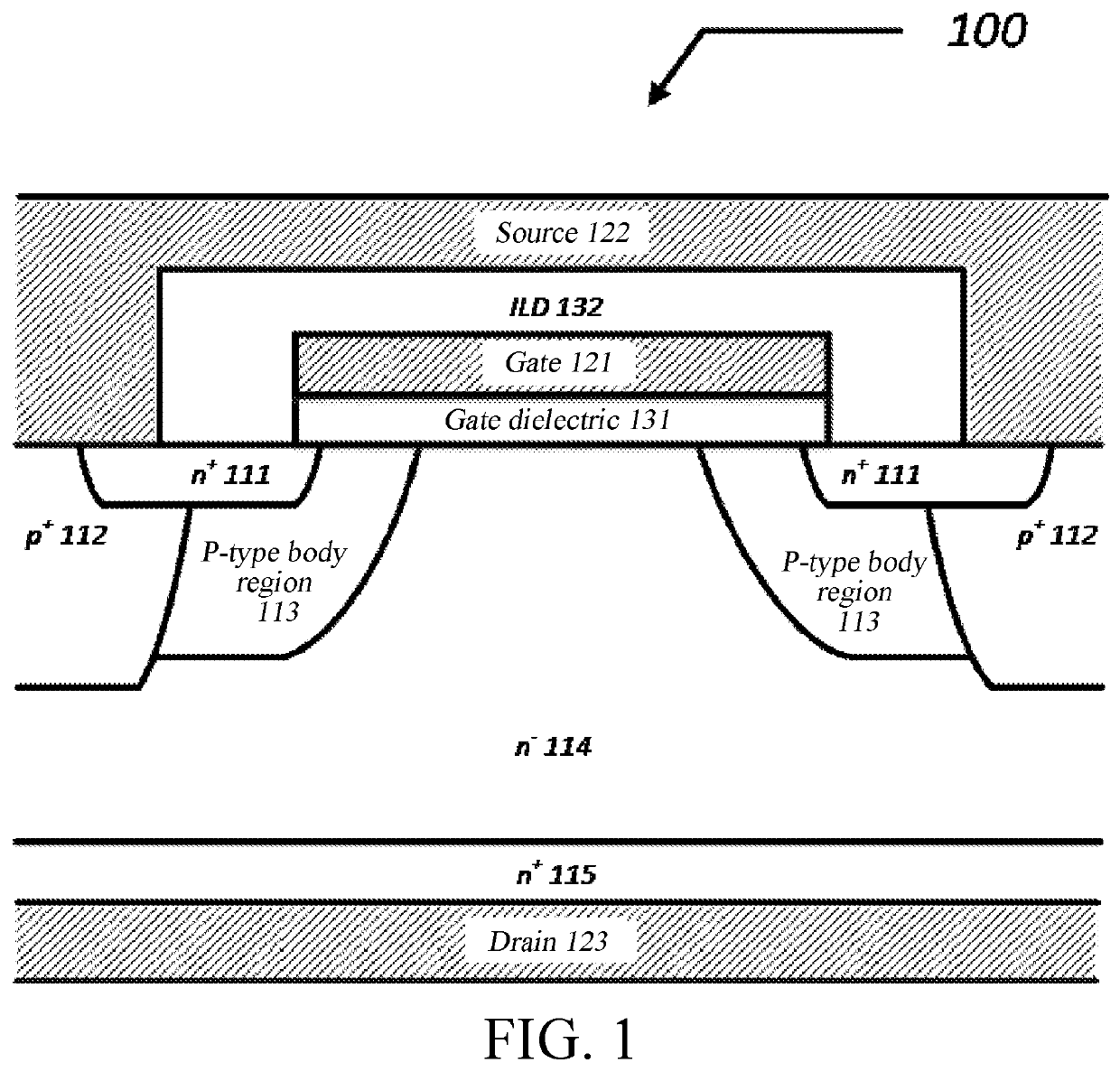
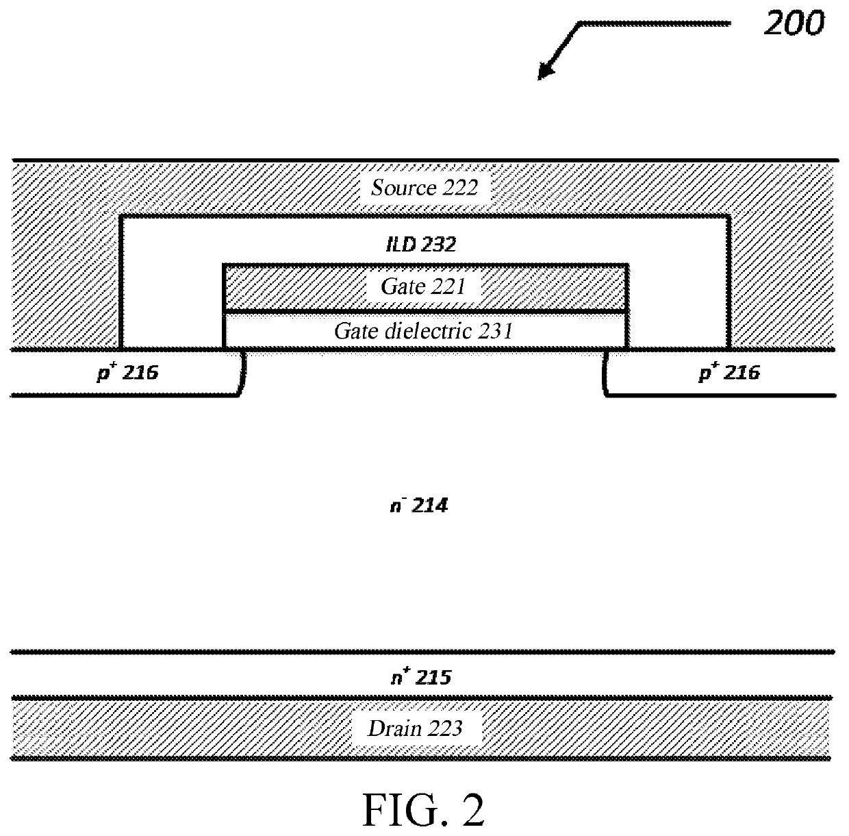
[0035]Please refer to FIG. 2. In the present embodiment, a drain electrode 223 is provided at the very bottom of the device 200 of the field effect transistor, an n+ drain 215 is provided at the top of the drain electrode 223, a n− drift region 214 is provided at the top of the n+ drain 215, a p+ source 216 is provided on part of the upper surface of the n− drift region 214, and in the present embodiment, there are two p+ sources 216 which are set symmetrically, and covering part of the upper surface of the n− drift region 214, a gate dielectric 231 is provided at the top of the n− drift region 214 and the p+ source 216, which covers above the n− drift region 214 and part of the top of the p+ source 216, a gate electrode 221 is provided at the top of the gate dielectric 231, an interlayer dielectric 232 (ILD) is provided at the top of the gate electrode 221, and in the present embodiment, the cross section of the interlayer dielectric 232 shows a “concave” shape, which covers above ...

embodiment 2

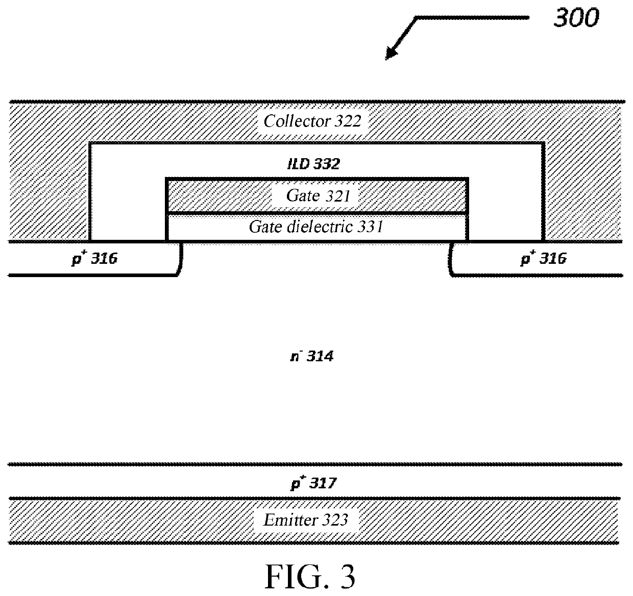
[0039]Please refer to FIG. 3. The present embodiment provides a gate-controlled PNP bipolar junction transistor (BJT). An emitter electrode 323 is provided at the very bottom of the body 300 of the field effect transistor, a p+ emitter 317 is provided at the top of the emitter electrode 323, a n− base 314 is provided at the top of the p+ emitter 317, a p+ collector 316 is provided on part of the upper surface of the n− base 314, and in the present embodiment, there are two p+ collectors 316 which are set symmetrically and cover part of the upper surface of the n− base 314, a gate dielectric 331 is provided at the top of the n− base 314 and the p+ collector 316, which covers above the n− base 314 and part of the top of the p+ collector 316, a gate electrode 321 is provided at the top of the gate dielectric 331, an interlayer dielectric 332 (ILD) is provided at the top of the gate electrode 321, in the present embodiment, the cross section of the interlayer dielectric 332 shows a “con...

embodiment 3

[0042]Please refer to FIG. 4. The structure of the present embodiment is similar to that of embodiment 1. In the present embodiment, a trench gate is provided in the n− drift region 414, and the gate dielectric 431 and the gate electrode 421 are located in the trench. The trench gate structure can lead to reduction in the gate distance between cells of the device and reduction of the on-resistance.


PUM

PropertyMeasurementUnit
lengthaaaaaaaaaa
lengthaaaaaaaaaa
depthaaaaaaaaaa

Abstract

The present invention discloses a rugged power semiconductor field effect transistor structure, and through a special design, it solves the problem that the activation under a transient condition may result in failures on the device, so that there is no parasitic BJT, and thus the device is more rugged.

Description

BACKGROUNDTechnical Field[0001]The present invention discloses a power semiconductor device structure, and in particular, relates to a rugged power semiconductor field effect transistor structure.Related Art[0002]Power semiconductor switching devices have been widely used in power electronic systems, such as switching power supplies and motor drives. In these applications, such devices are often required to be highly rugged. As shown in FIG. 1, a cross section of the structure of a prior art power semiconductor device is given. The device of the structure shown in FIG. 1 is commonly called as the vertical double diffused metal oxide semiconductor field effect transistor (i.e. VDMOS). A drain electrode 123 is provided at the very bottom of the device 100 of the field effect transistor. An n+ drain 115 (i.e. heavily doped n-type region drain) is provided at the top of the drain electrode 123. An n− drift region 114 (i.e. lightly doped n-type region drift region) is provided at the top...

Claims


Application Information

Patent Timeline
Patent Type & Authority Applications(United States)
IPC IPC(8): H01L29/08H01L29/78H01L29/06H01L29/10
CPCH01L29/0847H01L29/7802H01L29/0615H01L29/7816H01L29/1095H01L29/42312H01L29/739H01L29/7391
Inventor ZHAO, XIANDALIU, WAI YEESIN, JOHNNY KIN ON
Owner JSAB TECH (SHENZHEN) LTD
Why Eureka
Try Eureka