Display device and manufacturing method thereof

Inactive Publication Date: 2020-09-17
WUHAN CHINA STAR OPTOELECTRONICS SEMICON DISPLAY TECH CO LTD
View PDF0 Cites 4 Cited by
  • Summary
  • Abstract
  • Description
  • Claims
  • Application Information

AI Technical Summary

Benefits of technology

The patent describes a method of making a flexible display by creating a pattern in a buffer layer and attaching two layers of flexible substrate together through the pattern. This increases the contact area between the layers, reducing the risk of separation during bending. The technical effect is a more robust and reliable flexible display.

Problems solved by technology

However, for display devices with a two-layer organic polyimide film, the adhesion ability of the organic polyimide film to the inorganic layer is limited.

Method used


Image

  • Display device and manufacturing method thereof
  • Display device and manufacturing method thereof
  • Display device and manufacturing method thereof

Examples


Embodiment Construction

[0035]Structure and technical means adopted by the present disclosure to achieve the above and other objects can be best understood by referring to the following detailed description of the preferred embodiments and the accompanying drawings. Furthermore, directional terms described by the present disclosure, such as upper, lower, front, back, left, right, inner, outer, side, longitudinal / vertical, transverse / horizontal, etc., are only directions by referring to the accompanying drawings, and thus the used directional terms are used to describe and understand the present disclosure, but the present disclosure is not limited thereto.

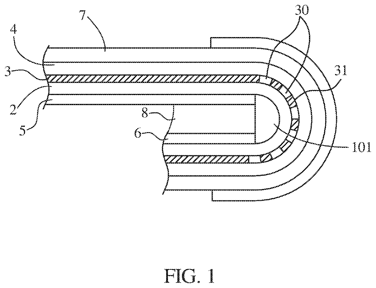
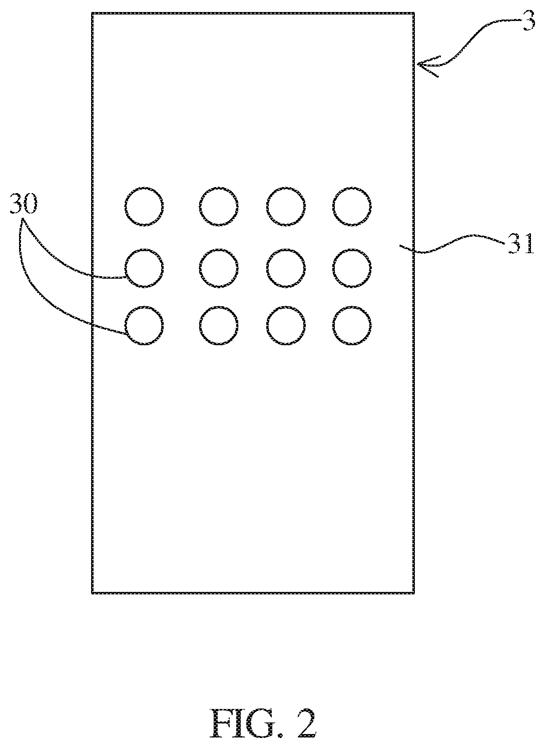
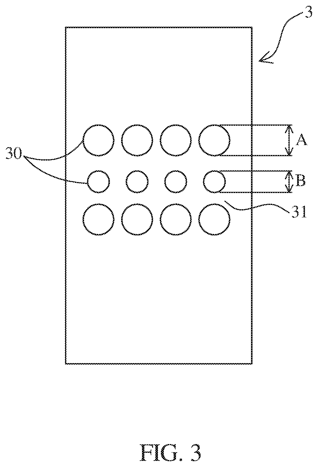
[0036]Referring to FIG. 1, a view of a display device according to a preferred embodiment of the present disclosure is illustrated. The display device includes a first flexible substrate layer 2, a buffer layer 3, a second flexible substrate layer 4, a first back plane 5, and a second back plane 6. The detailed structure of each component, assembly relati...


PUM


Abstract

A display device and a manufacturing method thereof are provided. The display device includes a first flexible substrate layer, at least one buffer layer, and a second flexible substrate layer, wherein the second flexible substrate layer is formed on the buffer layer, and the buffer layer is formed on the first flexible substrate layer; a bending region of the buffer layer is formed with a patterned pattern such that the first flexible substrate layer is attached to the second flexible substrate layer through the pattern.

Description

FIELD OF INVENTION[0001]The present disclosure relates to a display device, and in particular to a display device with an active matrix organic light emitting diode.BACKGROUND OF INVENTION[0002]Organic light emitting diode (OLED) displays are self-luminous displays. According to the driving method, they can be divided into passive matrix driving organic light emitting diode (PMOLED) displays and active matrix driving organic light emitting diode (AMOLED) displays. AMOLED displays have advantages, such as low manufacturing cost, fast response times, power savings, DC drive for portable devices, and a wide operating temperature range. Therefore, more and more AMOLED displays are used in a variety of displays with high performance.[0003]Further, in the display device of the AMOLED display, a first flexible substrate layer, a buffer layer and a second flexible substrate layer are disposed on a glass substrate. Then the glass substrate peeled by laser, and a back plane is attached, where...

Claims


Application Information

Patent Timeline
IPC IPC(8): H01L51/00H01L51/56
CPCH01L51/56H01L2251/5338H01L51/0097H10K59/127H10K77/111H10K59/1201H10K71/00Y02E10/549Y02P70/50H10K59/1275H10K2102/311
Inventor XIANG, MING
Owner WUHAN CHINA STAR OPTOELECTRONICS SEMICON DISPLAY TECH CO LTD
Why Eureka
Try Eureka