Semiconductor device and manufacturing method thereof

a technology of semiconductor devices and semiconductor shields, applied in semiconductor devices, diodes, electrical devices, etc., can solve the problems of reducing the esd resistance together with the lowering of current capacity, increasing the required area of protection diodes, and difficulty in reducing the size of semiconductor devices, so as to reduce the size of trenches and electrical characteristics. , to achieve the effect of suppressing the degradation of the esd resistance of the gate protection diodes, reducing the size o

Active Publication Date: 2020-10-01
ABLIC INC
View PDF0 Cites 4 Cited by
  • Summary
  • Abstract
  • Description
  • Claims
  • Application Information

AI Technical Summary

Benefits of technology

[0013]According to the present invention, independent setting of the thickness of the polysilicon layers enables the polysilicon layer for the protection diode and the polysilicon layer below a gate contact to be thick, and enables the polysilicon layer for the trench gate to have a film thickn...

Problems solved by technology

Thinning of the deposited polysilicon layer along with the reduction of the trench gate width, however, causes simultaneously thinning of the polysilicon layer of the protection diode made from the same polysilicon layer as the trench gate, resulting in lowering of the ESD resistance together with lowering of the current capacity.
To suppress the lowering of the ESD resistance, it is necessary to increase the PN junction area of the protection diode for the purpose of increasing the current capacity, however leading to an increase in the required area of the protection diode, thereby causing diff...

Method used


Image

  • Semiconductor device and manufacturing method thereof
  • Semiconductor device and manufacturing method thereof
  • Semiconductor device and manufacturing method thereof

Examples


Embodiment Construction

[0025]An embodiment of the present invention will hereinafter be described with reference to the accompanying drawings. The drawings used in the following description may be shown with being partly omitted, enlarged and seen through in order to make the features of the present invention easier to understand, and their dimension ratios may be different from the actual ones. Incidentally, the same components are denoted by the same reference numerals, and their duplicated explanations will be omitted as appropriate.

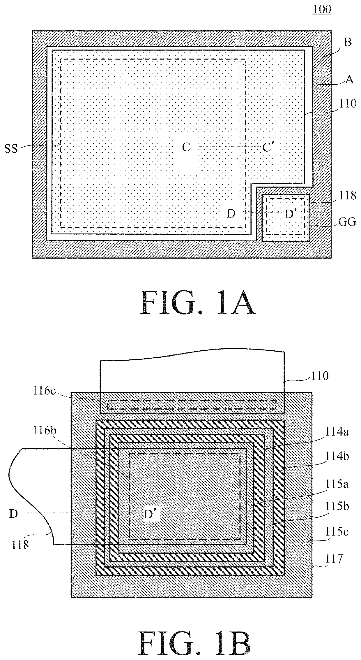
[0026]FIG. 1A is a schematic plan view to describe a semiconductor device 100 having a vertical MOSFET with trench gate according to the embodiment of the present invention. FIG. 1B is a schematic plan view showing the vicinity of a gate pad GG in FIG. 1A which is enlarged and partly seen through.

[0027]As illustrated in FIG. 1A, the semiconductor device 100 includes an active region A and a field region B provided along the perimeter of the active region A. The vertical MOS...


PUM


Abstract

A semiconductor device includes a semiconductor substrate, a trench provided in the semiconductor substrate, a trench gate formed in the trench, a vertical transistor having the trench gate, an active region having the vertical transistor, a field region surrounding the active region and having a protection diode, and a field insulating film formed on a surface of the semiconductor substrate, the protection diode being formed on the field insulating film. The trench gate includes a first polysilicon layer and has an embedded part embedded in the trench and an extension part connected to the embedded part and extending onto the surface of the semiconductor substrate, the protection diode includes a second polysilicon layer thicker than the first polysilicon layer, and an overlapping part having the second polysilicon layer is formed on the extension part.

Description

RELATED APPLICATIONS[0001]This application claims priority to Japanese Patent Application No. 2019-065171, filed on Mar. 29, 2019, the entire content of which is incorporated herein by reference.BACKGROUND OF THE INVENTION1. Field of the Invention[0002]The present invention relates to a semiconductor device, in particular to a semiconductor device having a gate protection diode and a vertical transistor which includes a trench gate and a gate insulating film.2. Description of the Related Art[0003]A semiconductor device having a vertical transistor which includes a gate insulating film usually has a gate protection diode which protects the gate insulating film from an ESD (Electro-Static Discharge) or the like. Such a protection diode is formed of a polysilicon film or the like provided on the insulating film and made from the same polysilicon layer which constitutes a gate.[0004]Japanese Patent Application Laid-open No. 2006-93505 discloses a technology in which a polysilicon layer ...

Claims


Application Information

Patent Timeline
IPC IPC(8): H01L29/78H01L29/06H01L29/417H01L29/66
CPCH01L29/7804H01L29/0611H01L29/41741H01L29/7813H01L29/66734H01L29/7827H01L29/4236H01L29/42364H01L27/0255H01L29/0869H01L29/861H01L29/16H01L29/7803
Inventor YOSHIMURA, MITSUHIRO
Owner ABLIC INC
Why Eureka
Try Eureka