Nonvolatile memory apparatus, write method of the nonvolatile memory apparatus, and system using the nonvolatile memory apparatus
- Summary
- Abstract
- Description
- Claims
- Application Information
AI Technical Summary
Benefits of technology
Problems solved by technology
Method used
Image


Examples
Embodiment Construction
[0014]Hereinafter, a semiconductor apparatus according to the present disclosure will be described below with reference to the accompanying drawings through various embodiments.
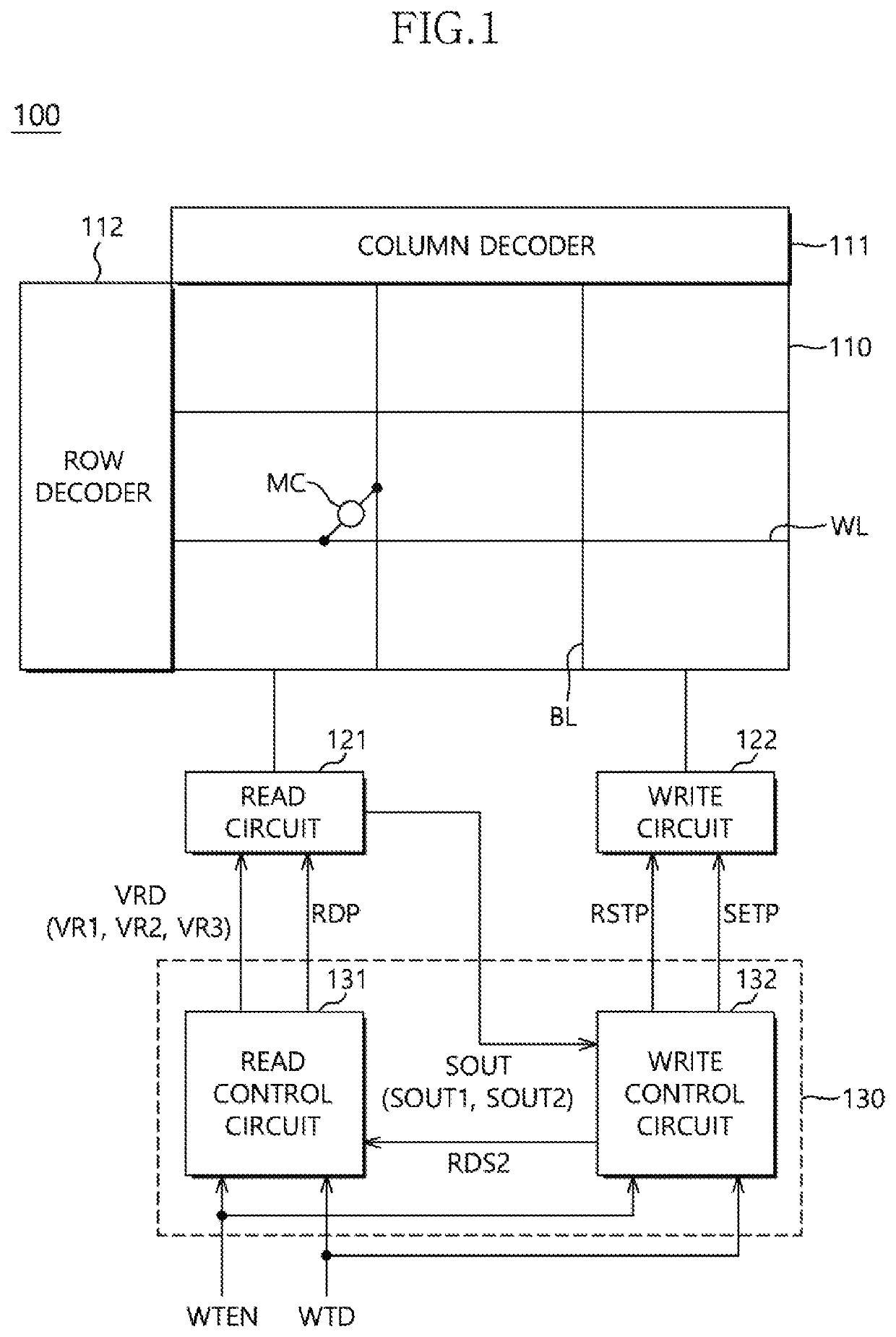
[0015]FIG. 1 is a diagram illustrating a configuration of a nonvolatile memory apparatus 100 in accordance with an embodiment. Referring to FIG. 1, the nonvolatile memory apparatus 100 may include a memory cell array 110. A plurality of bit lines BL may be disposed in a column direction within the memory cell array 110 and a plurality of word lines WL may be disposed in a row direction within the memory cell array 110. A plurality of memory cells MC may be respectively coupled to cross points between the plurality of bit lines BL and the plurality of word lines WL. Each of the memory cells MC may be electrically coupled between a corresponding bit line BL and a corresponding word line WL. The memory cell MC may be configured by a resistance change element, and, for example, may include a phase change material...
PUM
 Abstract
Description
Claims
Application Information