

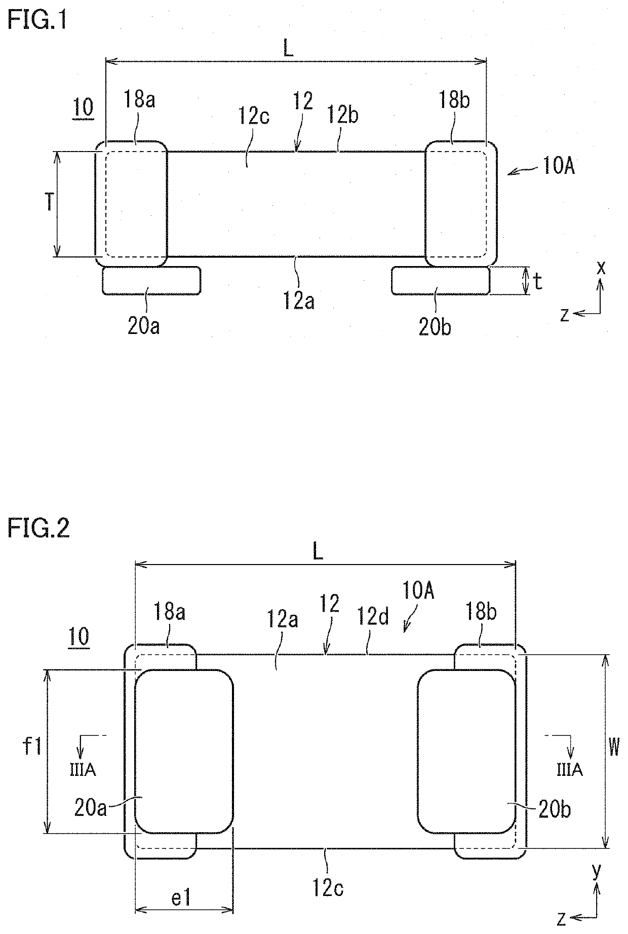
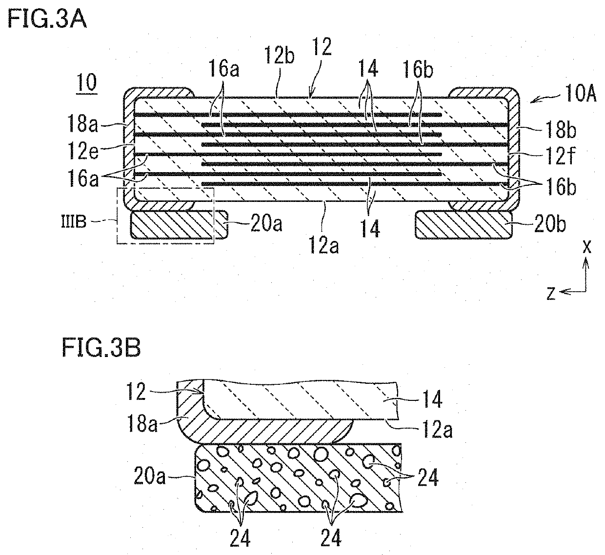
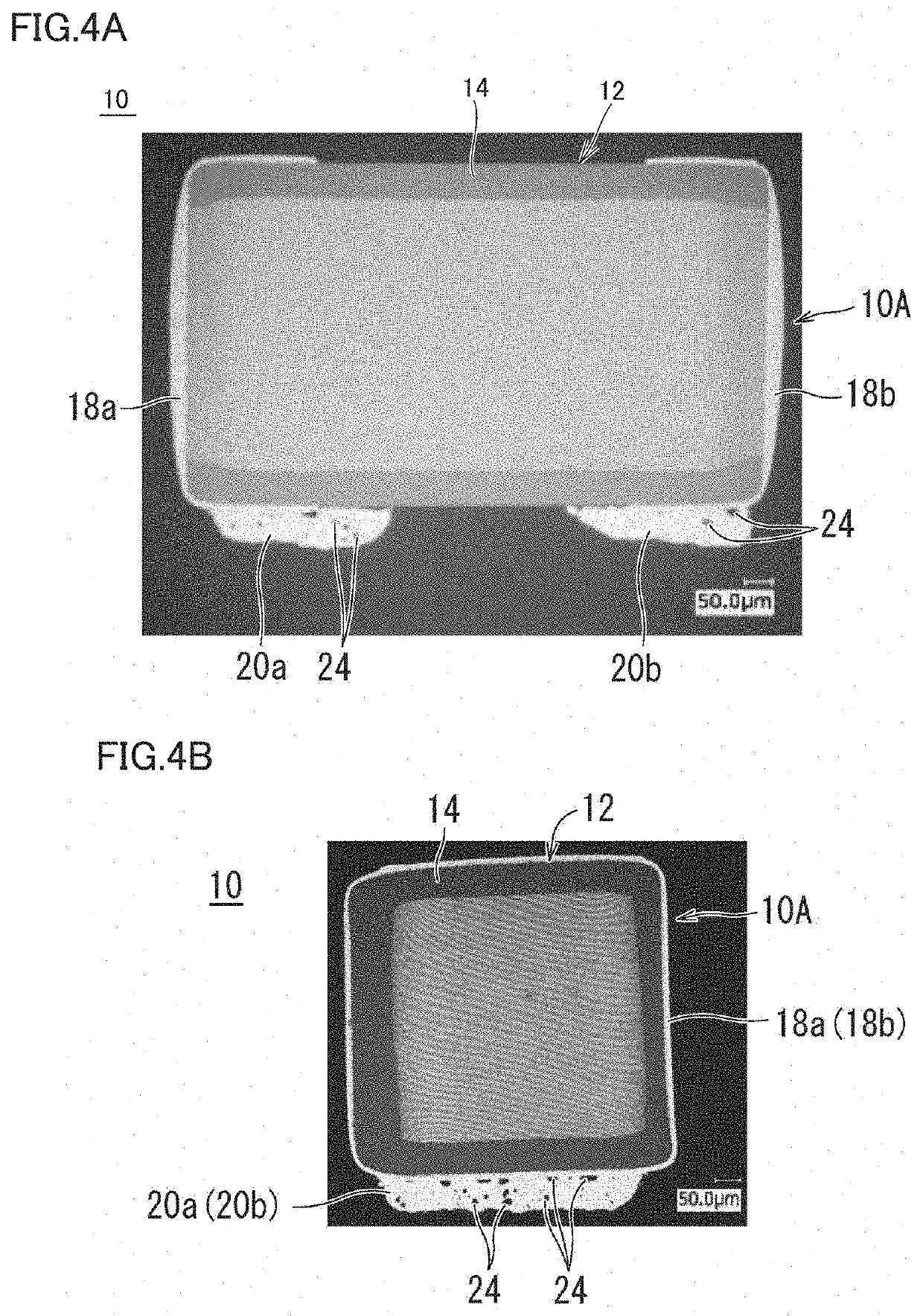
Chip electronic component and electronic component mounting structure
a technology of electronic components and mounting structures, which is applied in the direction of fixed capacitor details, stacked capacitors, fixed capacitors, etc., can solve the problems of interposer b>3/b> not being able to inhibit the wetting of solder, noise issues, etc., and achieve the desired mechanical strength, reduce the amount of solder, and prevent the wetting
- Summary
- Abstract
- Description
- Claims
- Application Information
AI Technical Summary
Benefits of technology
Problems solved by technology
Method used
Image

Examples
experimental example
5. Experimental Example
[0104]Next, an Experimental Example will be described, which was performed to confirm the “squeal” mitigation effects provided by a chip electronic component 10 included in the multilayer ceramic capacitor according to the present preferred embodiment.
(1) Sound Pressure Measurement Device
[0105]FIG. 14 shows a sound pressure measurement device 60 to measure the sound pressure level of noise generated by “squealing” of chip electronic component 1 included in the multilayer ceramic capacitor according to the present preferred embodiment. Referring to FIG. 14, mounting substrate 32 with chip electronic component 1 mounted thereon is installed in an anechoic box 62, while a sound collecting microphone 64 is disposed facing the mounting substrate 32. Then, an AC voltage having, for example, a frequency of about 3 kHz and a voltage of about 1 Vpp is applied to chip electronic component 10 included in the multilayer ceramic capacitor. This causes chip electronic compo...
PUM
| Property | Measurement | Unit |
|---|---|---|
| porosity | aaaaa | aaaaa |
| thickness | aaaaa | aaaaa |
| thickness | aaaaa | aaaaa |
Abstract
Description
Claims
Application Information