Image detection scanning method for object surface defects and image detection scanning system thereof
- Summary
- Abstract
- Description
- Claims
- Application Information
AI Technical Summary
Benefits of technology
Problems solved by technology
Method used
Image

Examples
Embodiment Construction
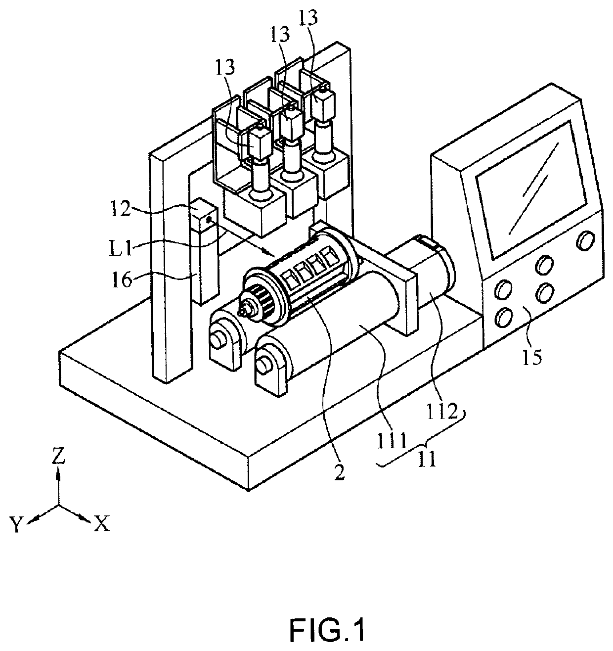
[0019]FIG. 1 shows a schematic diagram of an image detection scanning system for object surface defects according to an embodiment of the present disclosure. Referring to FIG. 1, the image detection scanning system for object surface defects is suitable for scanning an object 2 so as to obtain at least one detection image of the object 2. In some embodiments, the surface of the object 2 may include at least one surface defect, and the corresponding detection image also presents an image block with the surface defect. Herein, the surface defect is a three-dimensional structure. Herein, the three-dimensional structure is in a scale of mm to μm.
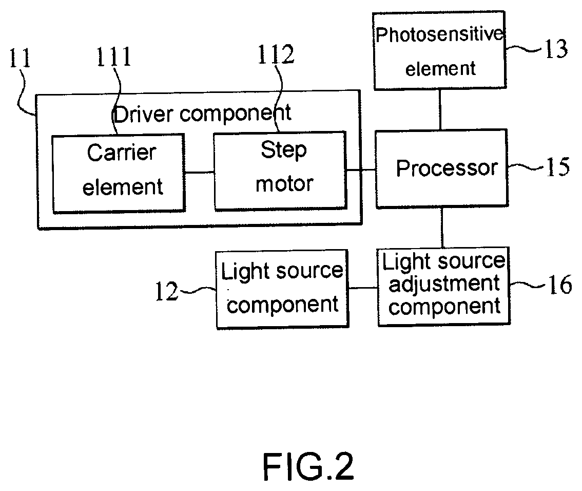
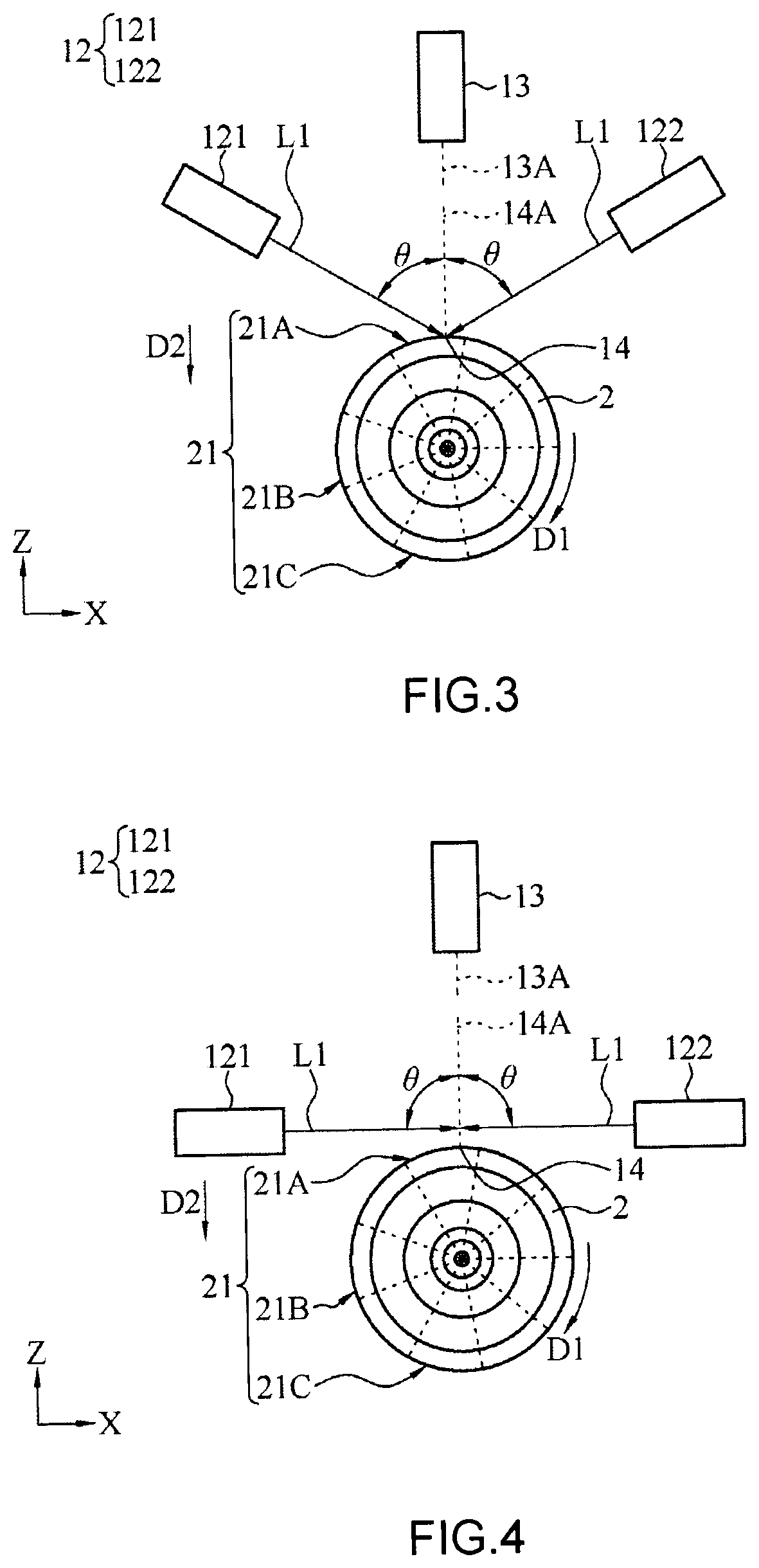
[0020]The image detection scanning system for object surface defects includes a driver component 11, a light source component 12 and a photosensitive element 13. Referring to FIG. 1 to FIG. 4, FIG. 2 shows a function block diagram of an image detection scanning system for object surface defects in FIG. 1 according to an embodiment, and FIGS. 3 a...
PUM
 Abstract
Description
Claims
Application Information
 - R&D Engineer
- R&D Manager
- IP Professional
- Industry Leading Data Capabilities
- Powerful AI technology
- Patent DNA Extraction
Browse by: Latest US Patents, China's latest patents, Technical Efficacy Thesaurus, Application Domain, Technology Topic.
© 2024 PatSnap. All rights reserved.Legal|Privacy policy|Modern Slavery Act Transparency Statement|Sitemap