

White light emitting diode and backlight module and display device comprising the same
- Summary
- Abstract
- Description
- Claims
- Application Information
AI Technical Summary
Benefits of technology
Problems solved by technology
Method used
Image

Examples
embodiment 1
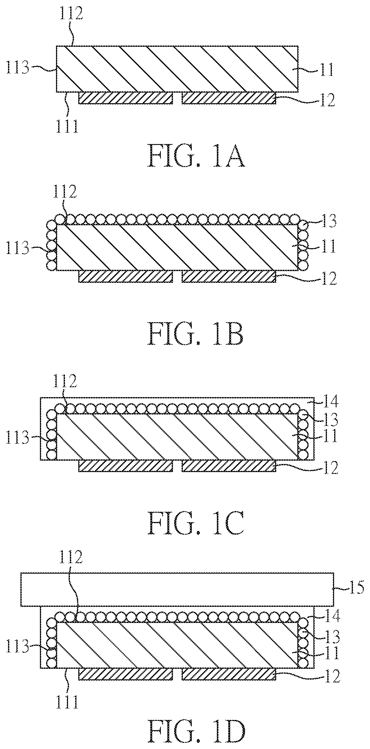
[0042]FIG. 1A to FIG. 1D are cross-sectional views showing a process for manufacturing a white light emitting diode according to the present embodiment.
[0043]As shown in FIG. 1A, a light emitting diode chip 11 is provided, which comprises a first surface 111 and a second surface 112 opposite to the first surface 111. Two electrodes 12 (respectively an anode and a cathode) are disposed on the first surface 111 of the light emitting diode chip 11. In addition, the light emitting diode chip 11 further comprises side surfaces 113 connecting to the first surface 111 and the second surface 112. In the present embodiment, the light emitting diode chip 11 is a flip-chip blue light emitting diode chip.
[0044]As shown in FIG. 1B, a phosphor layer 13 is formed on the second surface 112 and the side surfaces 113 of the light emitting diode chip 11. In the present embodiment, the method for forming the phosphor layer 13 is not particularly limited, and can be formed by the method disclosed in Tai...
embodiment 2
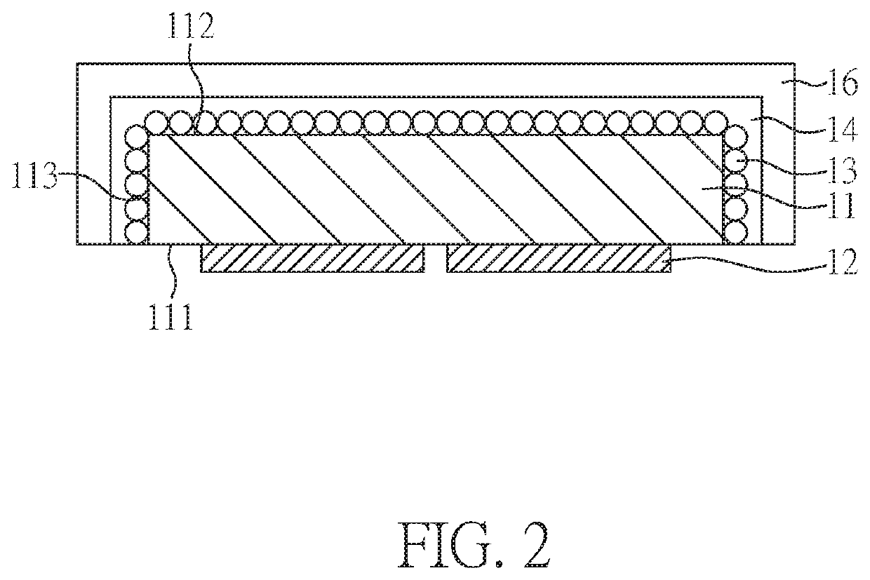
[0051]FIG. 2 is a cross-sectional view of a white light emitting diode according to the present embodiment. The preparing method and the structure of the white light emitting diode of the present embodiment are similar to those shown in Embodiment 1, except for the following differences.
[0052]In the present embodiment, the light filtering layer is formed on the protection layer via a coating process. Hence, in the present embodiment, in order to obtain the light filtering layer uniformly coated on the protection layer 14, a leveling process is performed on the protection layer 14 after forming the structure shown in FIG. 1C. Herein, a coating process known in the art (for example, a vacuum coating process) can be used to form a coating (not shown in the figure) on the protection layer 14 to level the surface of the protection layer 14. In the present embodiment, a Si3N4 film can be formed on the protection layer 14 via a plasma-enhanced chemical vapor deposition (PECVD), and the Si3...
embodiment 3
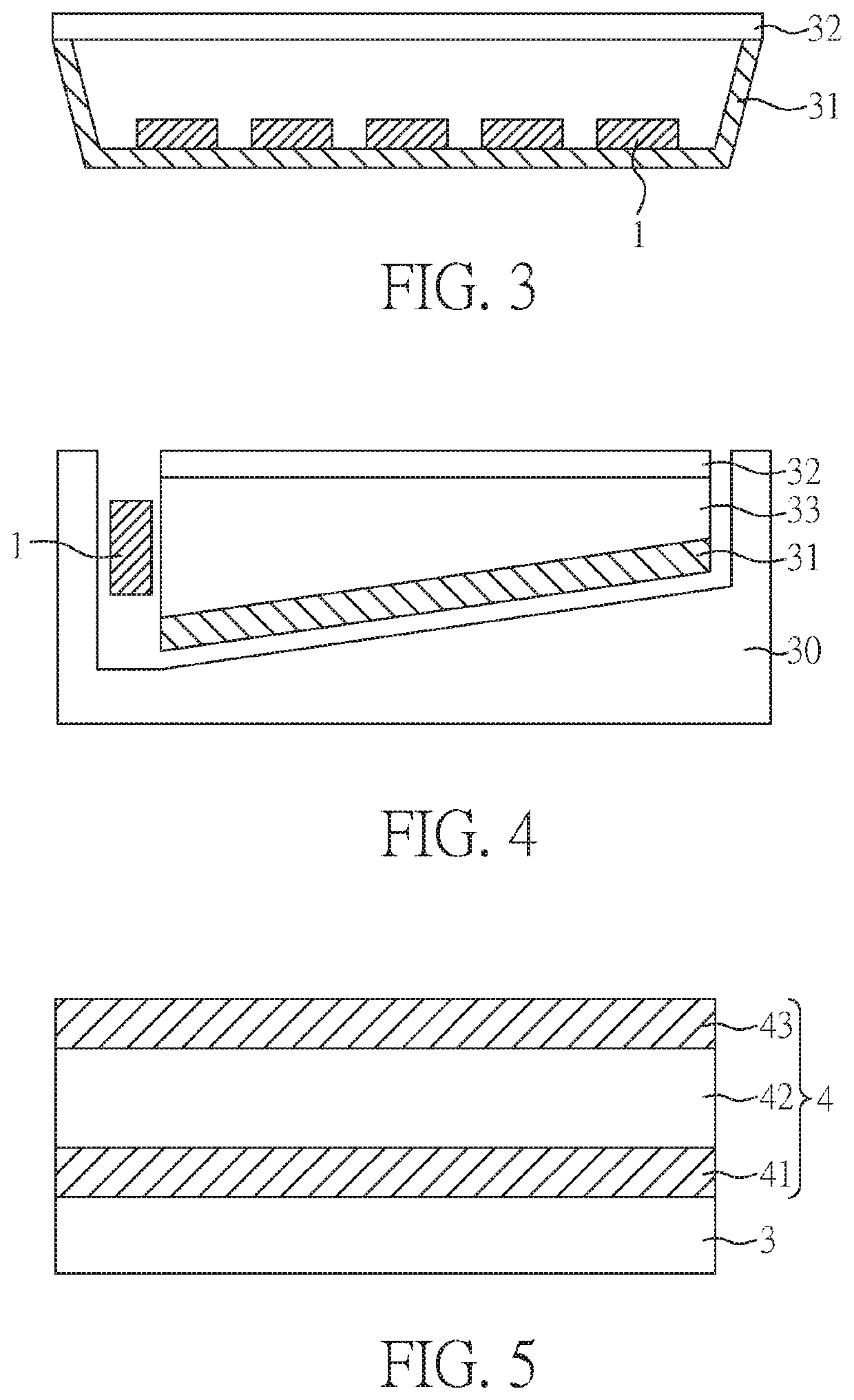
[0055]FIG. 3 is a cross-sectional view of a direct-light type backlight module according to the present embodiment. As shown in FIG. 3, the backlight module of the present embodiment comprises: a reflecting film 31; an optical film 32 disposed on the reflecting film 31; and a white light emitting diode 1 disposed between the reflecting film 31 and the optical film 32. In the present embodiment, the white light emitting diode 1 can be the white light emitting diode shown in Embodiment 1 or Embodiment 2.
[0056]In the present embodiment, the reflecting film 31 may be used as a house for the backlight module. In addition, even not shown in the figure, the optical film 32 may comprise conventional films used in the backlight module, for example, a diffusion film, a prism sheet or a brightness enhancement film. However, the present disclosure is not limited thereto, and the constitution of the optical film 32 can be adjusted according to the need.
PUM
 Abstract
Description
Claims
Application Information