Semiconductor light-emitting element

a technology light-emitting elements, which is applied in the direction of basic electric elements, electrical equipment, semiconductor devices, etc., can solve the problems of difficult to increase reflectivity, and achieve the effect of improving the light extraction efficiency of semiconductor light-emitting elements

Active Publication Date: 2020-12-17
NIKKISO COMPANY
View PDF0 Cites 3 Cited by
  • Summary
  • Abstract
  • Description
  • Claims
  • Application Information

AI Technical Summary

Benefits of technology

[0005]The present invention addresses the above-described issue, and an illustrative purpose thereof is to improve the light extraction efficiency of a semiconductor light-emitting element.
[0007]According to this embodiment, the area occupied by the active layer for improvement of light emission efficiency can be enlarged so that the light emission efficiency of the active layer can be improved, by configuring the area S1 in which the p-side contact electrode is formed to be larger than the area S2 in which the n-side contact electrode is formed. Meanwhile, it is not easy to increase the reflectivity R1 of the p-side contact electrode formed in a large area. The reflectivity R1 is constrained to be equal to lower than the reflectivity R2 of the n-side contact electrode formed in a small area. Under these conditions, the embodiment realizes a reflectivity of 50% or higher relative to the total area S0 of the substrate both in the n-side contact electrode and in the p-side contact electrode, reduces the loss incurred by absorption in the n-side or p-side contact electrode, and increases the light extraction efficiency of the element as a whole.

Problems solved by technology

Meanwhile, it is not easy to increase the reflectivity R1 of the p-side contact electrode formed in a large area.

Method used


Image

  • Semiconductor light-emitting element
  • Semiconductor light-emitting element
  • Semiconductor light-emitting element

Examples


Embodiment Construction

[0025]The invention will now be described by reference to the preferred embodiments. This does not intend to limit the scope of the present invention, but to exemplify the invention.

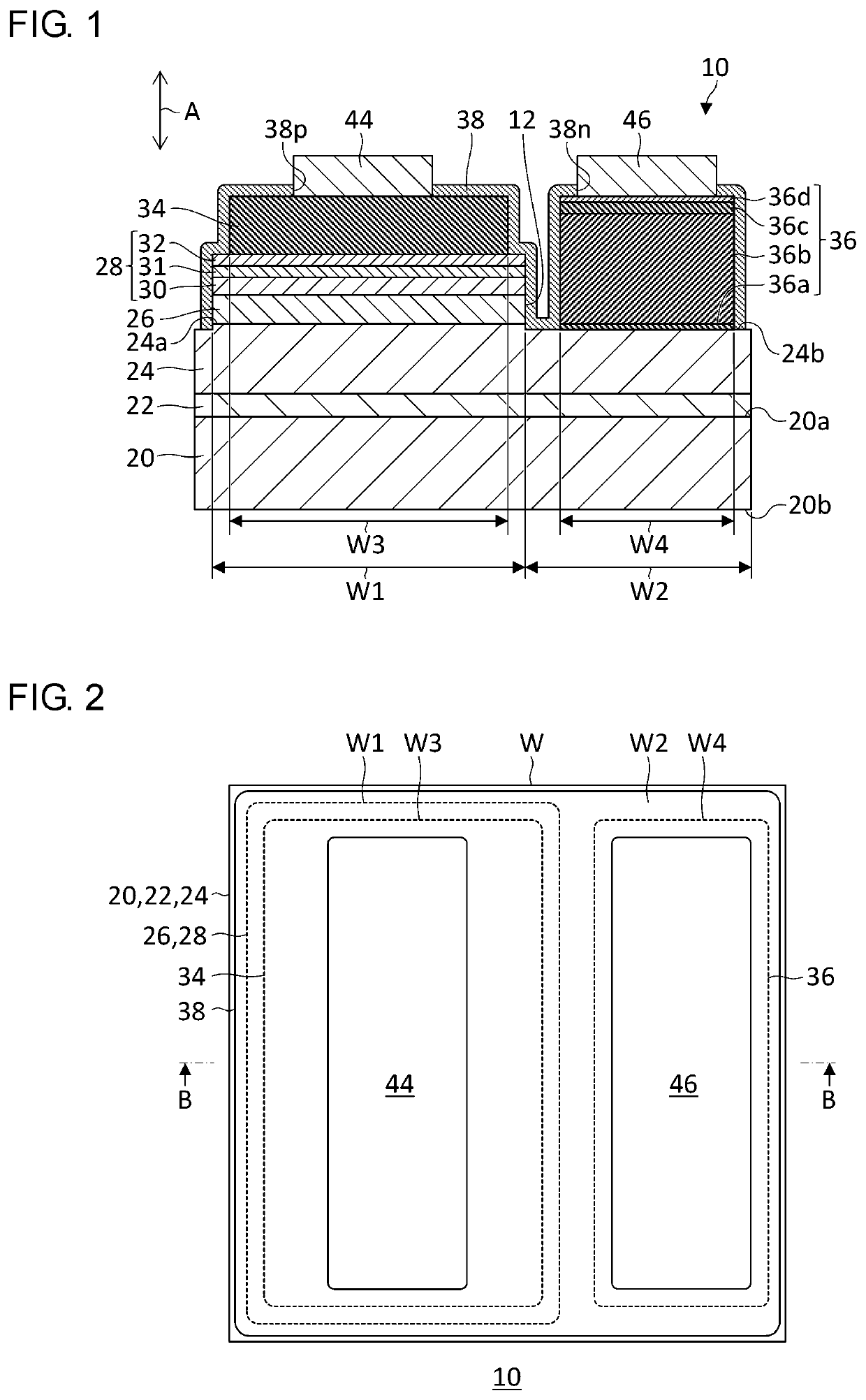
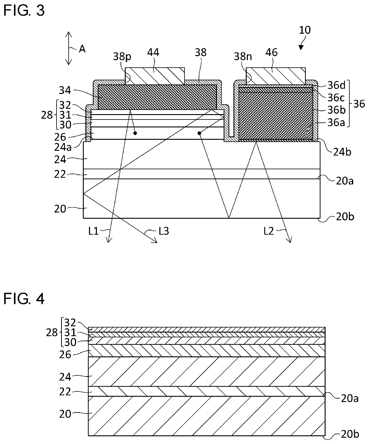
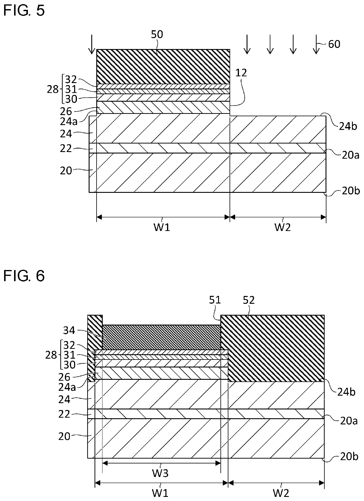
[0026]A detailed description will be given of embodiments of the present invention with reference to the drawings. The same numerals are used in the description to denote the same elements and a duplicate description is omitted as appropriate. To facilitate the understanding, the relative dimensions of the constituting elements in the drawings do not necessarily mirror the relative dimensions in the actual light-emitting element.

[0027]The embodiment relates to a semiconductor light-emitting element configured to emit “deep ultraviolet light” having a central wavelength λ of about 360 nm or shorter, which is a so-called deep ultraviolet-light emitting diode (DUV-LED). To output deep ultraviolet light having such a wavelength, an aluminum gallium nitride (AlGaN)-based semiconductor material having a band g...


PUM

PropertyMeasurementUnit
wavelengthaaaaaaaaaa
thicknessaaaaaaaaaa
thicknessaaaaaaaaaa

Abstract

A semiconductor light-emitting element is configured to emit ultraviolet light having a wavelength of 320 nm or shorter. Denoting a total area of a principal surface of a substrate as S0, an area on a p-type semiconductor layer in which a p-side contact electrode is formed as S1, an area on an n-type semiconductor layer in which an n-side contact electrode is formed as S2, a reflectivity of the p-side contact electrode for ultraviolet having a wavelength of 280 nm incident from a side of the p-type semiconductor layer as R1, and a reflectivity of the n-side contact electrode for ultraviolet light having a wavelength of 280 nm incident from a side of the n-type semiconductor layer as R2, (S1 / S0)×R1+(S2 / S0)×R2≥0.5, S1>S2, and R1≤R2.

Description

RELATED APPLICATION[0001]Priority is claimed to Japanese Patent Application No. 2019-108417, filed on Jun. 11, 2019, and Japanese patent Application No. 2019-189327, filed on Oct. 16, 2019, the entire contents of which are incorporated herein by reference.BACKGROUND OF THE INVENTION1. Field of the Invention[0002]The present invention relates to semiconductor light-emitting elements.2. Description of the Related Art[0003]A light-emitting element for emitting deep ultraviolet light having a wavelength of 355 nm or smaller includes an AlGaN-based n-type clad layer, an active layer, and a p-type clad layer stacked on a substrate. An p-side electrode of Ni / Au is provided on the p-type clad layer for obtaining ohmic contact. The p-side electrode of Ni / Au has a low reflectivity for deep ultraviolet light. Therefore, much of the deep ultraviolet light traveling from the active layer toward the p-side electrode is absorbed by the p-side electrode, resulting in lower light extraction efficien...

Claims


Application Information

Patent Timeline
Patent Type & Authority Applications(United States)
IPC IPC(8): H01L33/32H01L33/40H01L33/42
CPCH01L33/42H01L33/32H01L33/405H01L33/46
Inventor INAZU, TETSUHIKONIWA, NORITAKA
Owner NIKKISO COMPANY
Why Eureka
Try Eureka