Display assembly and display device

a technology of display device and assembly, which is applied in the field of display device, can solve the problems of reducing the efficiency of light emission

Pending Publication Date: 2021-01-07
HES IP HLDG LLC
View PDF0 Cites 0 Cited by
  • Summary
  • Abstract
  • Description
  • Claims
  • Application Information

AI Technical Summary

Benefits of technology

[0008]The purpose of the present invention is to provide an advantageous display

Problems solved by technology

The transistor and the capacitor may partially block the light e

Method used


Image

  • Display assembly and display device
  • Display assembly and display device
  • Display assembly and display device

Examples


Embodiment Construction

[0052]Embodiments of the present invention will now be described, by way of example only, with reference to the accompanying drawings.

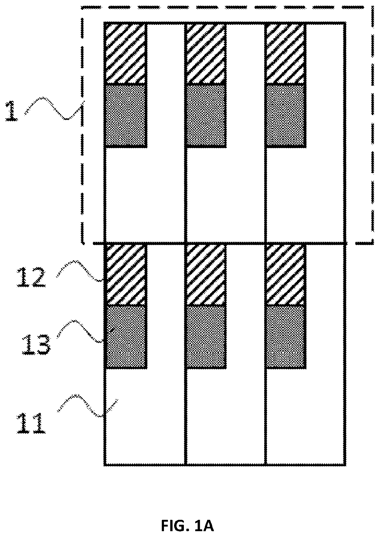
[0053]FIG. 1A illustrates a light emitting body 11, a transistor 12, and a capacitor 13 in a display assembly pixel 1 according to the prior art. When the light emitting body 11, the transistor 12 and the capacitor 13 are integrally provided, the light emitting body 11 will be partially blocked by the transistor 12 and the capacitor 13.

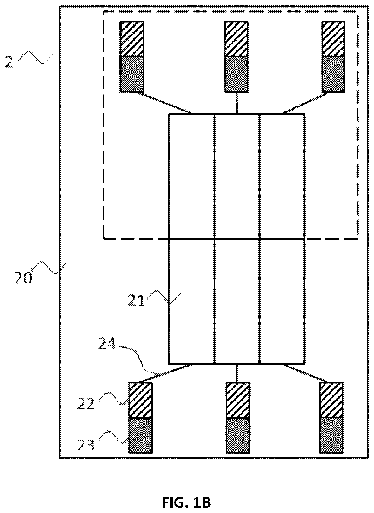
[0054]FIG. 1B illustrates a plurality of light emitting units 21 having a corresponding transistor unit 22 and a capacitor unit 23 of the display assembly 2 according to an embodiment of the present invention; in which the light emitting units 21, the transistor unit 22, and the capacitor unit 23 are independently provided on a side of a substrate 20. The light emitting units 21, the transistor unit 22, and the capacitor unit 23 are connected to a conductor 24. The light emitting units 21, the transistor unit 22 and the...


PUM


Abstract

Disclosed is a display assembly which comprises a substrate, a plurality of light emitting units, a transistor unit and a capacitor unit corresponding to each of the plurality of light emitting units. Each of the plurality of light emitting units is electrically coupled to the corresponding transistor unit and the capacitor unit, all of which are independently provided on a side of the substrate. A spacing between each of the plurality of light emitting units is at least two times of a first threshold length.

Description

CROSS-REFERENCE TO RELATED APPLICATIONS[0001]This non-provisional application claims priority under 35 U.S.C. § 119(a) on Patent Application No(s). PCT / CN2018 / 077715 on Mar. 1, 2018, the entire contents of which are hereby incorporated by reference.FIELD OF THE INVENTION[0002]The present invention is related to a display assembly; more particularly, a display device comprising the display assembly.BACKGROUND OF THE INVENTION[0003]As the demand for real-time information rises, the importance of on-demand data transmission is also increased. Near-eye displays (NED) can be easily incorporated into other devices and can transmit images, colors, texts and / or sound data at any time; therefore, it is a primary choice for portable information device or on-demand data transmission purposes. Near-eye displays are often implemented for military or governmental uses in the past. Currently, the near-eye display industry seeks expansion in the consumer sector. Meanwhile, the entertainment industr...

Claims


Application Information

Patent Timeline
IPC IPC(8): H01L27/32H01L25/16G02B27/01
CPCH01L27/3218H01L25/167H01L51/5275H01L27/3244G02B27/0172H01L25/0753H01L33/58G02B3/0006G02B2027/0127H10K59/353H10K59/879H01L27/15H10K59/121H10K59/123H10K59/35H10K59/50G02B27/01G02F1/294G02B27/30G02F1/29G02F2203/12G02F2203/24G02F2203/28H10K50/858H10K59/12
Inventor CHEN, TAI KUO
Owner HES IP HLDG LLC
Why Eureka
Try Eureka