Structure including a photoresist underlayer and method of forming same

a technology of photoresist and underlayer, which is applied in the field of structures and methods of forming the same, can solve the problems of inconvenient deposited sog, inconvenient forming of the same, and difficulty in forming sog at a thickness of less than 10 nm, etc., and achieves the effect of improving the uniformity of deposited sog

Pending Publication Date: 2021-01-14
ASM IP HLDG BV
View PDF6 Cites 174 Cited by
  • Summary
  • Abstract
  • Description
  • Claims
  • Application Information

AI Technical Summary

Benefits of technology

[0009]Various embodiments of the present disclosure relate to structures including improved photoresist underlayers (sometimes referred to as adhesion layers) and to methods of forming the layers and structures. While the ways in which various embodiments of the present disclosure address drawbacks of prior methods and structures are discussed in more detail below, in general, various embodiments of the disclosure provide structures that can include a relatively thin, uniform photoresist underlayer with desired properties, such as desired etch selectivity, pattern quality, and / or stability.

Problems solved by technology

Unfortunately, it can be difficult to deposit SOG at a thickness of less than 10 nm.
Further, a within substrate and substrate-to-substrate thickness non-uniformity of deposited SOG can be undesirably high, particularly as a target thickness of the SOC layer is reduced.

Method used


Image

  • Structure including a photoresist underlayer and method of forming same
  • Structure including a photoresist underlayer and method of forming same
  • Structure including a photoresist underlayer and method of forming same

Examples


Embodiment Construction

[0058]Although certain embodiments and examples are disclosed below, it will be understood by those in the art that the invention extends beyond the specifically disclosed embodiments and / or uses of the invention and obvious modifications and equivalents thereof. Thus, it is intended that the scope of the invention disclosed should not be limited by the particular disclosed embodiments described below.

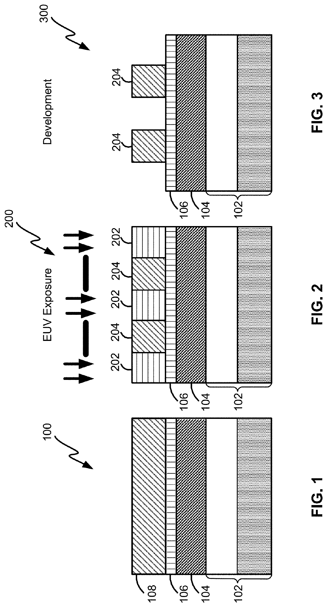
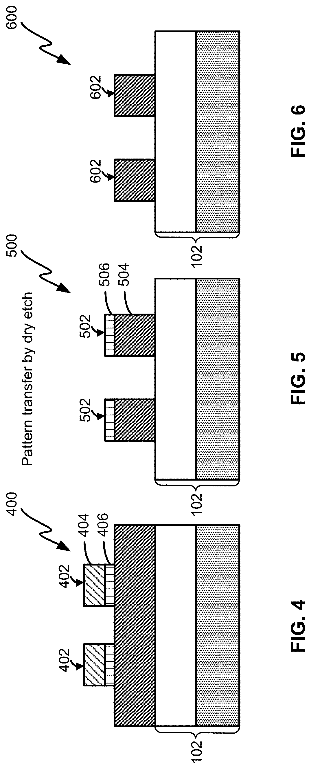
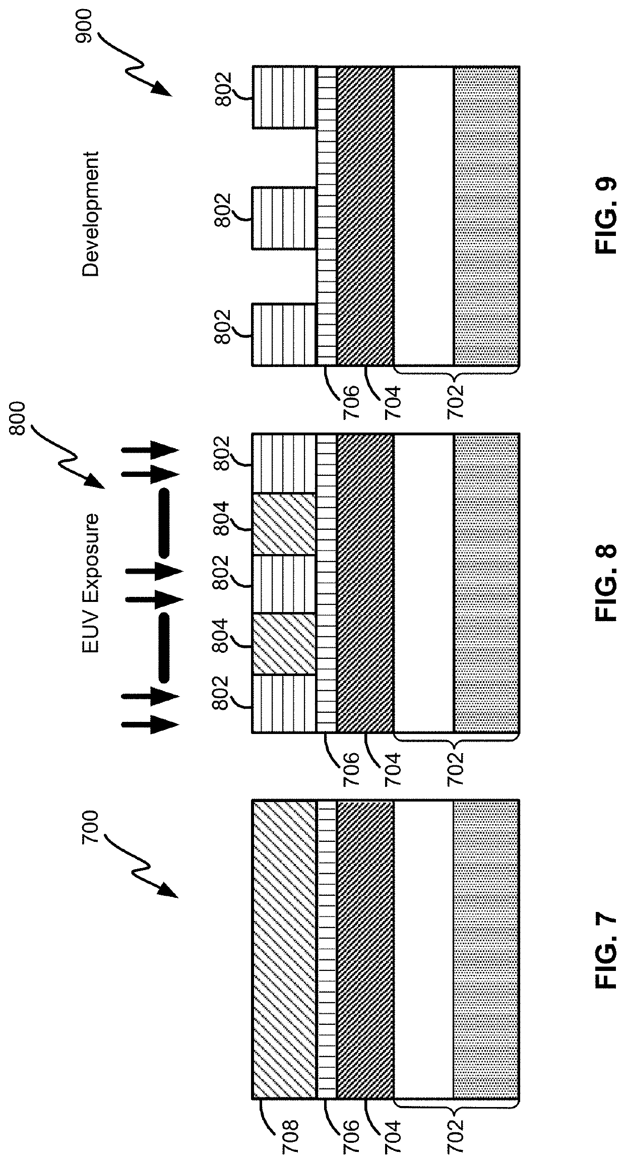
[0059]The present disclosure generally relates to methods of forming structures that include a photoresist underlayer and to structures including a photoresist underlayer. As described in more detail below, exemplary methods can be used to form structures with photoresist underlayers that provide desired properties, such as desired thickness (e.g., less than 10 or less than 5 nm), relatively low surface roughness, good adhesion to the photoresist, desired etch selectivity, desired thickness uniformity—both within a substrate (e.g., a wafer) and between substrates, high pattern quality ...


PUM

PropertyMeasurementUnit
thicknessaaaaaaaaaa
surface energyaaaaaaaaaa

Abstract

Methods of forming structures including a photoresist underlayer and structures including the photoresist underlayer are disclosed. Exemplary methods include forming the photoresist underlayer using one or more of plasma-enhanced cyclic (e.g., atomic layer) deposition and plasma-enhanced chemical vapor deposition. Surface properties of the photoresist underlayer can be manipulated using a treatment process.

Description

CROSS-REFERENCE TO RELATED APPLICATIONS[0001]This application claims priority to U.S. Provisional Patent Application Ser. No. 62 / 872,239 filed Jul. 9, 2019 titled STRUCTURE INCLUDING A PHOTORESIST UNDERLAYER AND METHOD OF FORMING SAME, the disclosures of which are hereby incorporated by reference in their entirety.FIELD OF INVENTION[0002]The present disclosure generally relates to structures and to methods of forming the structures. More particularly, the disclosure relates to structures including a photoresist underlayer and to methods of forming such structures.BACKGROUND OF THE DISCLOSURE[0003]During the manufacture of electronic devices, fine patterns of features can be formed on a surface of a substrate by patterning the surface of the substrate and etching material from the substrate surface using, for example, gas-phase etching processes. As a density of devices on a substrate increases, it becomes increasingly desirable to form features with smaller dimensions.[0004]Photores...

Claims


Application Information

Patent Timeline
Patent Type & Authority Applications(United States)
IPC IPC(8): H01L21/033H01L21/311G03F7/20G03F7/38
CPCH01L21/0332G03F7/38G03F7/70033H01L21/31144G03F7/0752G03F7/16G03F7/167G03F7/094H01L21/02126H01L21/02216H01L21/02274H01L21/0228H01L21/0234G03F7/11G03F7/0755G03F7/0382G03C1/74G03F7/004G03F7/095
Inventor SUN, YITINGDE ROEST, DAVIDPIUMI, DANIELERAAIJMAKERS, IVO JOHANNESKIM, BOKHEONBLANQUART, TIMOTHEETOMCZAK, YOANN
Owner ASM IP HLDG BV
Why Eureka
Try Eureka