Light-emitting device and capacitor

a light-emitting device and capacitor technology, applied in the direction of stacked capacitors, semiconductor lasers, thin/thick film capacitors, etc., can solve the problems of inability to shorten the pulse of light, difficult to output light with a desired pulse width, and certain time, so as to achieve the effect of reducing the inductance of parasitic materials

Active Publication Date: 2021-01-28
MURATA MFG CO LTD
View PDF11 Cites 4 Cited by
  • Summary
  • Abstract
  • Description
  • Claims
  • Application Information

AI Technical Summary

Benefits of technology

[0009]The present disclosure provides a light-emitting device that achieves shortening of the pulse of light to be output and a capacitor that achieves shortening of the pulse of light to be output from a solid-state light-emitting element placed in the capacitor.
[0012]According to the present disclosure, a solid-state light-emitting element and a switching element are connected in series and are placed on an outer face of a capacitor. Therefore, parasitic inductance can be reduced, and light with a short pulse can thus be output from the solid-state light-emitting element.

Problems solved by technology

Therefore, the pulse width of output light is fixed, and it is thus difficult to output light with a desired pulse width.
However, the parasitic inductance restricts the rising speed of current of the laser diode, and there thus arises a problem of requiring a certain time or more to achieve a suitable current value.
That is, even with the light-emitting device using the switch control method, only light with a certain pulse width or more can be output, and shortening the pulse of light cannot be achieved.
As a result, the ON duration during which light is output from the light-emitting device is restricted to a value more than several ns, and there thus arises a problem of not being able to ensure a sufficient range resolution.

Method used


Image

  • Light-emitting device and capacitor
  • Light-emitting device and capacitor
  • Light-emitting device and capacitor

Examples


first embodiment

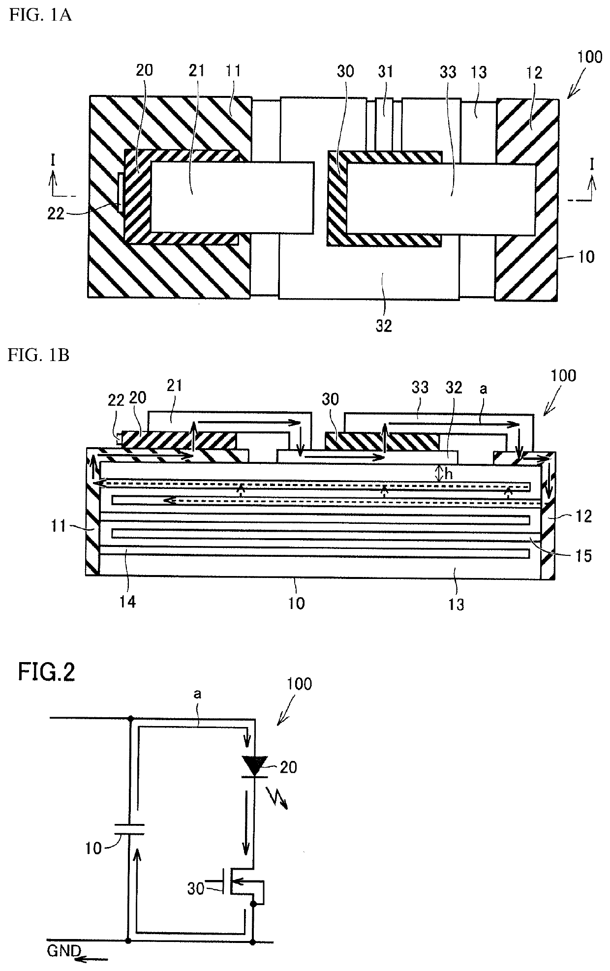
[0038]A light-emitting device according to a first embodiment of the present disclosure will be described below with reference to drawings. FIGS. 1A and 1B include schematic diagrams for explaining a configuration of a light-emitting device 100 according to the first embodiment of the present disclosure. FIG. 1A is a plan view of the light-emitting device 100 when viewed from an outer face of a capacitor 10 on which a solid-state light-emitting element 20 is placed, and FIG. 1B is a cross-section view of the light-emitting device 100 taken along plane I-I.

[0039]The light-emitting device 100 illustrated in FIGS. 1A and 1B include the capacitor 10, and the solid-state light-emitting element 20 and a semiconductor switch 30 that are placed on the outer face of the capacitor 10. The capacitor 10 is a capacitor for electric power supply and is a multilayer ceramic capacitor. Thus, in the capacitor 10, a plurality of inner electrodes 14 and 15 for acquiring electrostatic capacitance and a...

second embodiment

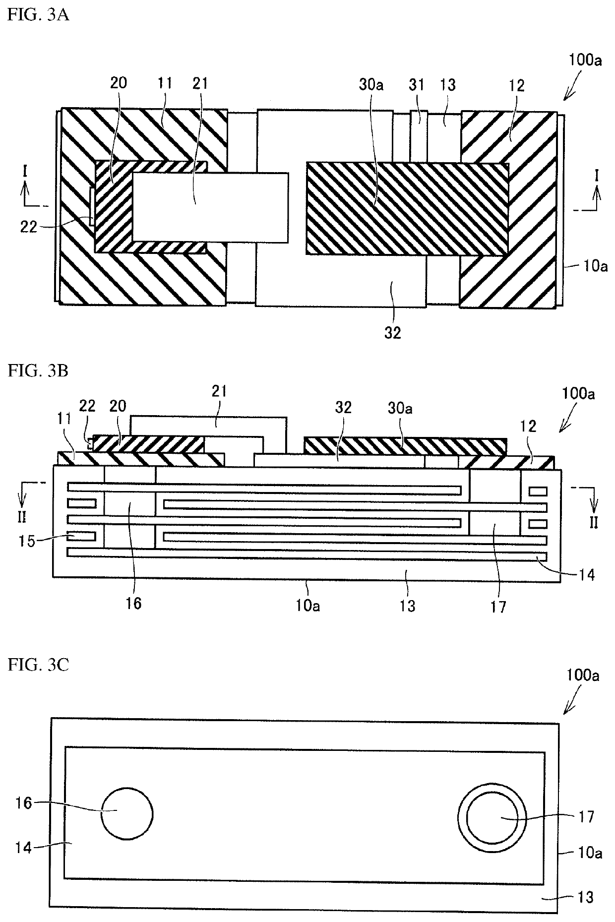
[0052]In the light-emitting device 100 according to the first embodiment, as illustrated in FIG. 1B, the outer electrodes 11 and 12 are formed in the corresponding end portions of the multilayer body, and the size of the current loop a is under the constraint of the external size of the capacitor 10. Thus, in a second embodiment of the present disclosure, a configuration is used in which an outer electrode and an inner electrode are electrically connected using a via conductor for a capacitor. FIGS. 3A, 3B, and 3C include schematic diagrams for explaining a configuration of a light-emitting device 100a according to the second embodiment of the present disclosure. FIG. 3A is a plan view of the light-emitting device 100a when viewed from the outer face of a capacitor 10a on which the solid-state light-emitting element 20 is placed, FIG. 3B is a cross-section view of the light-emitting device 100a taken along plane I-I, and FIG. 3C is a cross-section view of the light-emitting device 1...

third embodiment

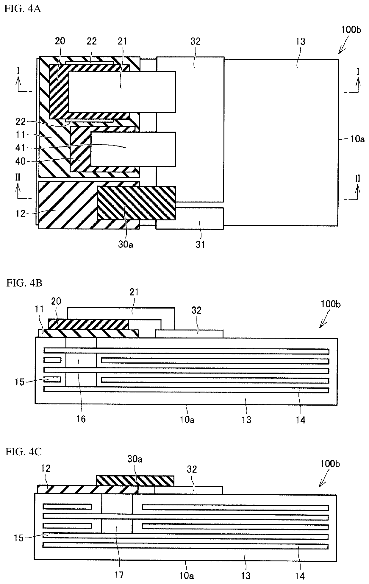
[0061]The configuration of the light-emitting device 100 according to the first embodiment that includes the capacitor 10, and the solid-state light-emitting element 20 and the semiconductor switch 30 that are placed on the outer face of the capacitor 10 has been described above. However, elements placed on the outer face of the capacitor are not limited to the solid-state light-emitting element and the semiconductor switch. In a third embodiment of the present disclosure, a configuration in which elements other than the solid-state light-emitting element and the semiconductor switch are placed on the outer face of the capacitor will be described.

[0062]FIGS. 4A, 4B, and 4C include schematic diagrams for explaining a configuration of a light-emitting device 100b according to a third embodiment of the present disclosure. FIG. 4A is a plan view of the light-emitting device 100b when viewed from the outer face of the capacitor 10a on which the solid-state light-emitting element 20 is pl...


PUM

PropertyMeasurementUnit
distanceaaaaaaaaaa
thicknessaaaaaaaaaa
thicknessaaaaaaaaaa

Abstract

The present disclosure provides a light-emitting device that is able to output light with a shorter pulse. A light-emitting device according to the present disclosure includes a capacitor, one or more solid-state light-emitting elements that emit light when electric power is supplied from the capacitor, and a semiconductor switch that controls electric power supply from the capacitor to the solid-state light-emitting element. Furthermore, the solid-state light-emitting element is placed on an outer face of the capacitor, the semiconductor switch is placed on the outer face of the capacitor or provided inside the capacitor, and the capacitor includes a connecting electrode between outer electrodes, the connecting electrode allowing the solid-state light-emitting element and the semiconductor switch to be connected in series.

Description

[0001]This is a continuation of International Application No. PCT / JP2019 / 007021 filed on Feb. 25, 2019, which claims priority from Japanese Patent Application No. 2018-084615 filed on Apr. 26, 2018 and Japanese Patent Application No. 2018-122000 filed on Jun. 27, 2018. The contents of these applications are incorporated herein by reference in their entireties.BACKGROUNDTechnical Field[0002]The present disclosure relates to a light-emitting device that includes one or more solid-state light-emitting elements and a capacitor on which one or more solid-state light-emitting elements may be placed.[0003]Nowadays, LiDAR (Light Detection and Ranging) may be used for automotive systems, meteorological observation systems, and the like. The LiDAR includes a light-emitting device, which is described in Non-Patent Document 1, including a laser diode, a semiconductor switch, a clamp diode, a capacitor for electric power supply, and the like.[0004]Driving methods of light-emitting devices includ...

Claims


Application Information

Patent Timeline
Patent Type & Authority Applications(United States)
IPC IPC(8): H01L25/16H01S5/042H05B33/08H05B45/40H01S5/0239H05B44/00
CPCH01L25/167H01S5/042H01G4/30H05B45/40H05B33/08H01G4/40H01G4/33H05B45/30H01S5/0239H05B44/00
Inventor TAKIMOTO, NAOMIMATSUOKA, TAKAHIROKUSHIMA, TAKAHITOOHARA, TATSUYAANDO, SHOTANAKANO, HIROYUKI
Owner MURATA MFG CO LTD
Why Eureka
Try Eureka