Filter element
- Summary
- Abstract
- Description
- Claims
- Application Information
AI Technical Summary
Benefits of technology
Problems solved by technology
Method used
Image

Examples
first preferred embodiment
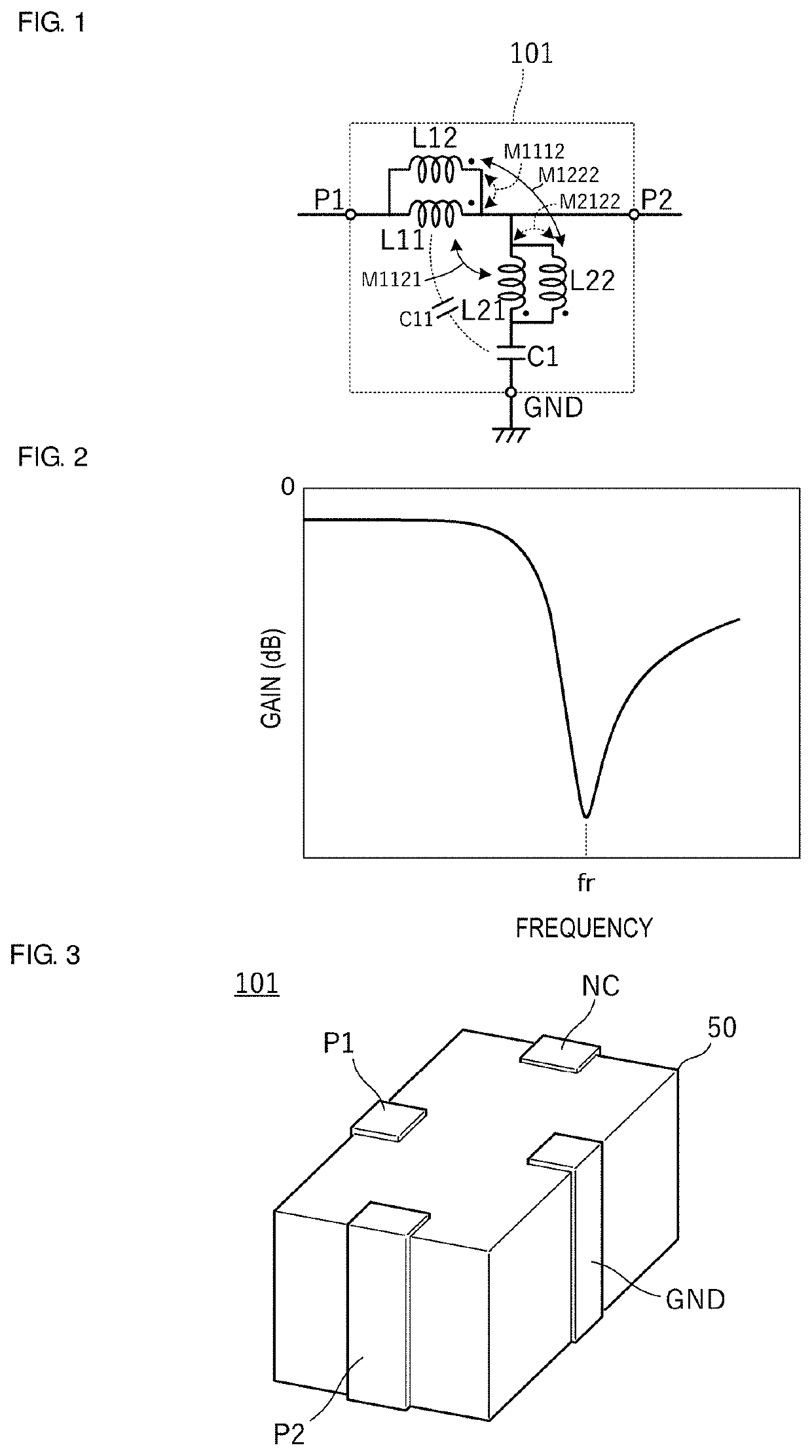
[0041]FIG. 1 is a circuit diagram of a filter element 101 according to a first preferred embodiment of the present invention. FIG. 2 is a graph indicating a frequency characteristic of the insertion loss of the filter element 101.
[0042]The filter element 101 includes input-output terminals P1 and P2 and a ground terminal GND. The input-output terminals P1 and P2 are provided in series on a signal path and the ground terminal GND is grounded.
[0043]In the filter element 101, inductors L11 and L12 that are connected in parallel to each other are connected in series to the signal path. In addition, a series circuit including a parallel circuit of inductors L21 and L22 that are connected in parallel to each other and a capacitor C1 is shunt-connected between the signal path and ground.
[0044]The inductors L11 and L12 correspond to “series inductors” and the inductors L21 and L22 correspond to “shunt inductors”. The inductor L11 corresponds to a “first series inductor” and the inductor L12...
second preferred embodiment
[0067]An example of a filter element is described in a second preferred embodiment of the present invention, which includes capacitor conductive patterns different from those in the first preferred embodiment.
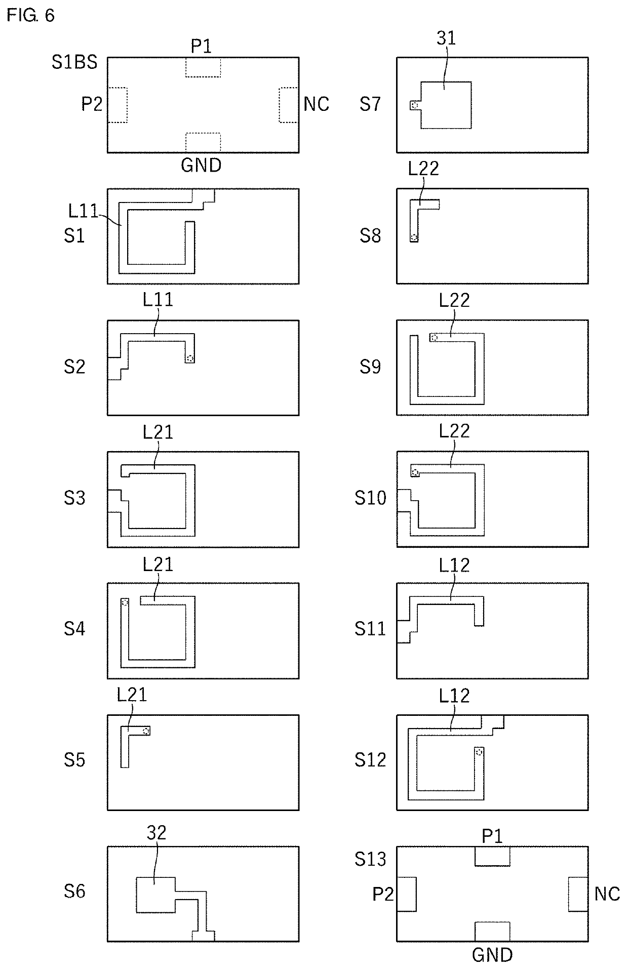
[0068]FIG. 9 illustrates a vertical cross section of a filter element 102 according to the second preferred embodiment. FIG. 10 is a plan view of multiple insulating layers of the filter element 102.
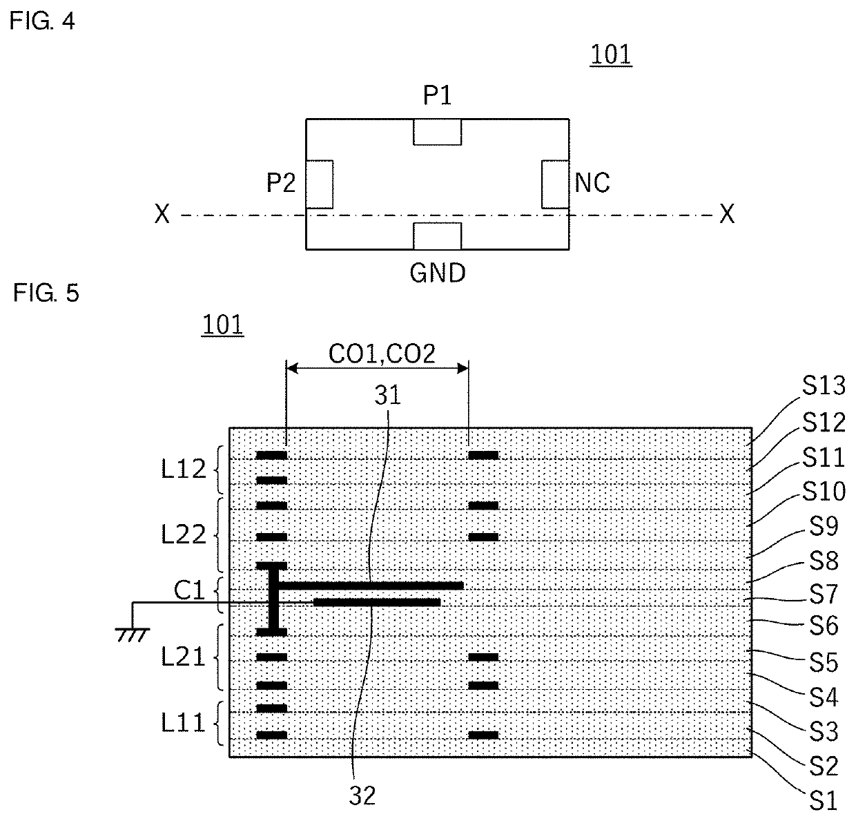
[0069]Referring to FIG. 10, the inductor conductive patterns and the capacitor conductive patterns are provided on the upper surfaces of the insulating layers S1 to S10. The insulating layer SIBS represents the conductive pattern on the lower surface of the insulating layer S1 in FIG. 10. The input-output terminals P1 and P2, the ground terminal GND, and the free terminal NC are provided on the lower surface of the insulating layer S1 and the upper surface of the insulating layer S10. The first series inductor L11 is provided on the upper surfaces of the insulating layers S1 and S2,...
third preferred embodiment
[0074]Circuits are described in a third preferred embodiment of the present invention, in which another filter circuit is connected downstream of a filter element defining and functioning as a low pass filter.
[0075]FIG. 11A is a circuit diagram of a circuit in which a band elimination filter 201 is connected downstream of the filter element 101. FIG. 11B is a circuit diagram explicitly indicating the mutual inductance occurring in the filter element 101 as a circuit element.
[0076]FIG. 12A is a circuit diagram of a circuit in which a band elimination filter 202 is connected downstream of the filter element 101. FIG. 12B is a circuit diagram explicitly indicating the mutual inductance occurring in the filter element 101 as a circuit element.
[0077]The band elimination filter 201 is a circuit in which a parallel circuit of an inductor L3 and a capacitor C2 is connected in series to the signal path. The band elimination filter 202 is a circuit in which the parallel circuit of the inducto...
PUM
 Abstract
Description
Claims
Application Information
 - R&D Engineer
- R&D Manager
- IP Professional
- Industry Leading Data Capabilities
- Powerful AI technology
- Patent DNA Extraction
Browse by: Latest US Patents, China's latest patents, Technical Efficacy Thesaurus, Application Domain, Technology Topic.
© 2024 PatSnap. All rights reserved.Legal|Privacy policy|Modern Slavery Act Transparency Statement|Sitemap