Semiconductor packages having package-on-package (POP) structures

a technology of semiconductors and packages, applied in the field of semiconductor packages, to achieve the effect of reducing non-wetting problems, increasing the size of individual solder balls, and preventing and/or reducing non-wetting problems

Active Publication Date: 2021-04-08
SAMSUNG ELECTRONICS CO LTD
View PDF0 Cites 1 Cited by
  • Summary
  • Abstract
  • Description
  • Claims
  • Application Information

AI Technical Summary

Benefits of technology

[0004]Therefore, the present disclosure has been made in view of the above problems, and it is an object of the present disclosure to provide a semiconductor package having a PoP structure, in which a power connector region and a signal connector region are formed separately from each other such that the power connector is disposed on the top surface of an upper semiconductor package and the signal connector is disposed on the bottom surface of the upper semiconductor package, thereby increasing the size of an individual solder ball, preventing and / or reducing a non-wetting problem, which may occur upon arrangement of a plurality of signal connectors and power connectors in a limited space, increasing the number of signal connectors, and thus increasing the bandwidth of data transmission.

Problems solved by technology

However, reducing the size of the individual terminals and reducing the pitch between the terminals may cause a non-wetting problem in which the terminals are disconnected from each other.

Method used


Image

  • Semiconductor packages having package-on-package (POP) structures
  • Semiconductor packages having package-on-package (POP) structures
  • Semiconductor packages having package-on-package (POP) structures

Examples


Embodiment Construction

[0024]Reference will now be made in detail to the embodiments of the present disclosure, examples of which are illustrated in the accompanying drawings. Wherever possible, the same reference numbers will be used throughout the drawings to refer to the same or like parts.

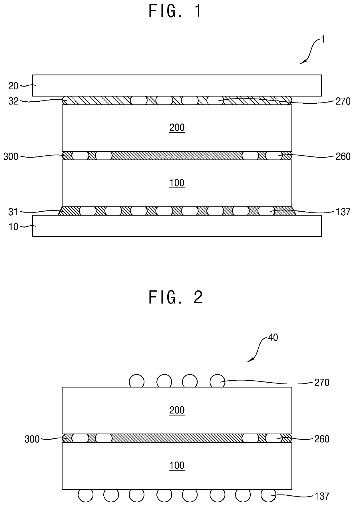
[0025]FIG. 1 is a side cross-sectional view of a semiconductor system 1 according to an embodiment of the present disclosure. Referring to FIG. 1, a semiconductor system 1 according to an embodiment of the present disclosure may include a lower board 10, an upper board 20, a lower underfill 31, an upper underfill 32, a lower semiconductor package 100, an upper semiconductor package 200, and a package underfill 300. The lower semiconductor package 100 may include a solder 137 disposed on the bottom surface thereof (e.g., between the lower semiconductor package 100 and the lower board 10). The upper semiconductor package 200 may include a signal connector 260 disposed on the bottom surface thereof (e.g., between the up...


PUM

PropertyMeasurementUnit
diameteraaaaaaaaaa
semiconductor packageaaaaaaaaaa
sizeaaaaaaaaaa

Abstract

Disclosed is a semiconductor package having a package-on-package (PoP) structure in which a signal region and a power region are formed separately. The semiconductor package includes a lower semiconductor package and an upper semiconductor package on the lower semiconductor package. The upper semiconductor package includes an upper package substrate, a memory chip on the upper package substrate, a wire that electrically connects the memory chip to the upper package substrate, a power connector on the upper semiconductor package, a signal connector on the bottom surface of the upper package substrate, and an upper package molding material.

Description

CROSS-REFERENCE TO RELATED APPLICATION[0001]This application claims the benefit of priority under 35 USC § 119 to Korean Patent Application No. 10-2019-0122969, filed on Oct. 4, 2019, in the Korean Intellectual Property Office, the entire contents of which are incorporated herein by reference.BACKGROUND1. Field[0002]Example embodiments relate to semiconductor packages. More particularly, example embodiments relate to semiconductor packages having a package-on-package (PoP) structure.2. Description of Related Art[0003]In the case of a semiconductor package having a PoP structure, the number of signal connectors may be increased in order to increase the bandwidth of data transmission between an upper semiconductor package and a lower semiconductor package of the PoP structure. In a conventional semiconductor package having a PoP structure, power connectors and signal connectors are disposed together in the limited space between the upper semiconductor package and the lower semiconduct...

Claims


Application Information

Patent Timeline
Patent Type & Authority Applications(United States)
IPC IPC(8): H01L25/065H01L23/00H01L23/498H01L23/31
CPCH01L25/0657H01L24/45H01L23/3121H01L23/49816H01L24/13H01L23/49838H01L23/3128H01L25/071H01L2224/16227H01L2924/15311H01L2924/15192H01L2224/73227H01L2224/48227H01L2224/32145H01L2224/73265H01L2225/06517H01L2225/0651H01L2225/06558H01L2225/06562H01L2225/06524H01L2225/1023H01L2225/1058H01L2225/107H01L25/105H01L25/0652H01L25/50H01L25/18H01L2224/04105H01L2224/73267H01L2924/00H01L24/46H01L24/49H01L24/14H01L24/17H01L23/525H01L23/481H01L23/31
Inventor HONG, MINGI
Owner SAMSUNG ELECTRONICS CO LTD
Why Eureka
Try Eureka