Radio frequency connectors, omni-directional WIFI antennas, omni-directional dual antennas for universal mobile telecommunications service, and related devices, systems, methods, and assemblies

a technology of omni-directional wifi antennas and connectors, applied in the field of physical and conductive coupling circuits and device components, can solve the problems of inadequate transmission and/or reception of radio waves by the antenna construction and/or arrangement, and achieve the effect of ensuring the transmission and/or reception of radio waves as desired

Active Publication Date: 2021-04-22
RLSMITH HLDG LLC
View PDF3 Cites 7 Cited by
  • Summary
  • Abstract
  • Description
  • Claims
  • Application Information

AI Technical Summary

Benefits of technology

[0010]Some advantageous antenna systems can have an RF connector, a PCB dipole antenna, and / or a radome. The RF connector provides a direct connection to the PCB and limits PIM. An omni-directional WiFi antenna has a pair of horizontal dipole antennas on a PCB having different wavelengths and same frequency. An omni-directional UMTS dual antenna has a vertical arrangement of two independent antennas on a PCB and has a jumper printed circuit board connecting the RF connector to the upper antenna. Corresponding connectors, radomes, and ways of combining antenna elements on a single PCB are also disclosed. A single frequency omnidirectional antenna includes both half and full wavelength dipole elements. A plus-shaped radome enhances the omnidirectional radiation pattern of the enclosed antenna. A jumper printed circuit board allows independent antennas on a single circuit board without the degradation of internal coaxial connections. The connector provides a direct interface with a circuit board to reduce the number of parts and also reduce passive intermodulation.
[0015]In some applications, a radio frequency connector comprises a pin configured to carry a radio frequency signal. Ground arms are positioned on opposing sides of the pin. The ground arms are configured to connect with respective ground connections of a printed circuit board. Each of the ground arms comprises a first portion arranged to contact the printed circuit board. A second portion is arranged to be spaced apart from the printed circuit board when the first portion is in contact with the printed circuit board. The ground arms are shaped to provide thermal relief while the radio frequency connector is being soldered to the printed circuit board.
[0017]In some applications, a radio frequency connector comprises a conductive body. At least one pair of conductive arms each configured to provide an electrical connection between the conductive body and ground pads of a printed circuit board (PCB). The at least one pair of conductive arms further configured to hold the PCB therebetween. Each of the conductive arms comprises at least one cutout that provides thermal relief when a heat source is applied to an end of the conductive arm configured to contact the PCB. A center pin is configured to electrically contact a trace on the PCB and communicate a signal with the trace. An insulator is configured to electrically isolate the center pin from the at least one pair of conductive arms and the conductive body. A connector portion is configured to couple the at least one pair of conductive arms, the center pin, the conductive body, and the insulator to a device.
[0019]In some applications, an apparatus for transmitting data and / or power wirelessly comprises a printed circuit board (PCB) comprising a transmission line and a ground trace electrically isolated from the transmission line. A radio frequency connector comprises a conductive body. At least one pair of conductive arms is each configured to provide an electrical connection between the conductive body and ground pads of a printed circuit board (PCB). The at least one pair of conductive arms further configured to hold the PCB therebetween. Each of the conductive arms comprises at least one cutout that provides thermal relief when a heat source is applied to an end of the conductive arm configured to contact the PCB. A center pin is configured to electrically contact a trace on the PCB and communicate a signal with the trace. An insulator is configured to electrically isolate the center pin from the at least one pair of conductive arms and the conductive body.

Problems solved by technology

In some applications, the construction and / or arrangement of the antenna does not adequately transmit and / or receive radio waves as desired.

Method used


Image

  • Radio frequency connectors, omni-directional WIFI antennas, omni-directional dual antennas for universal mobile telecommunications service, and related devices, systems, methods, and assemblies
  • Radio frequency connectors, omni-directional WIFI antennas, omni-directional dual antennas for universal mobile telecommunications service, and related devices, systems, methods, and assemblies
  • Radio frequency connectors, omni-directional WIFI antennas, omni-directional dual antennas for universal mobile telecommunications service, and related devices, systems, methods, and assemblies

Examples


Embodiment Construction

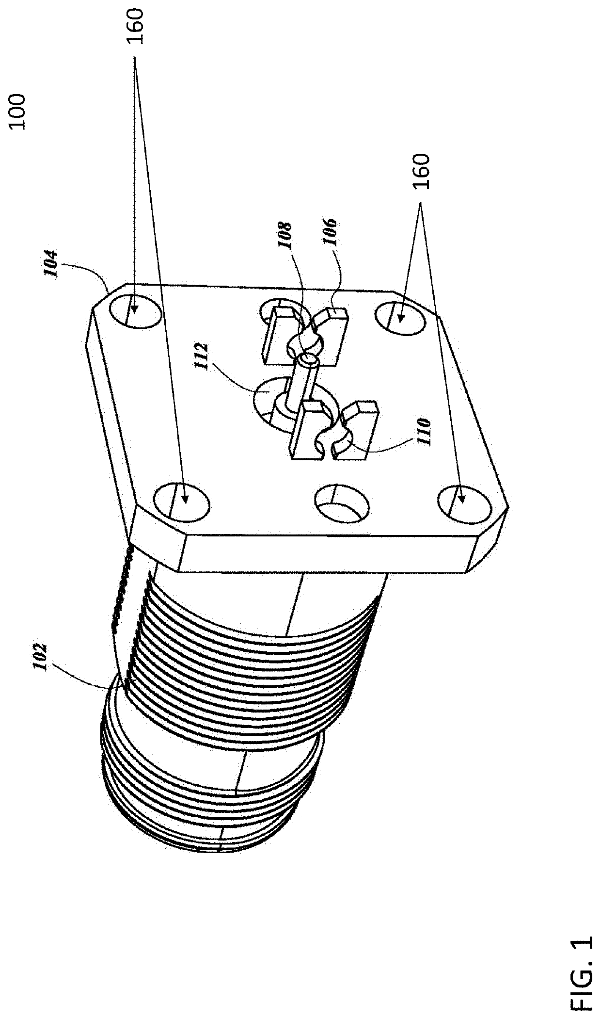
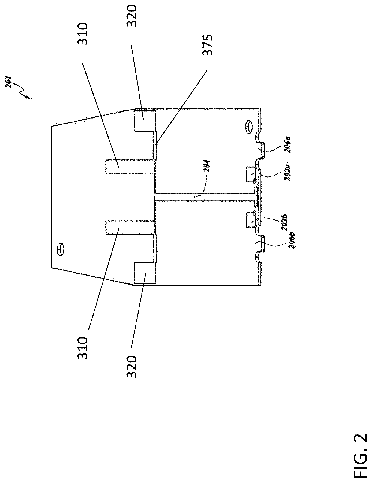
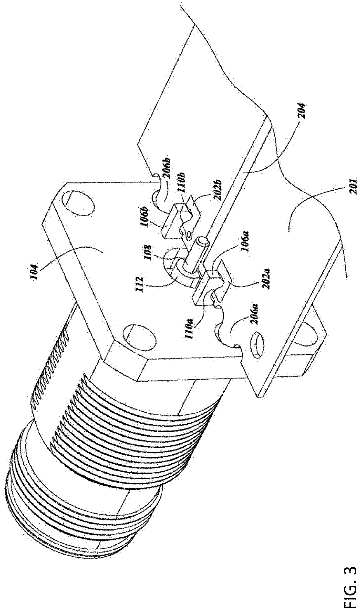
[0080]The following detailed description of certain embodiments presents various descriptions of specific embodiments. However, the innovations described herein can be embodied in a multitude of different ways, for example, as defined and covered by the claims. In this description, reference is made to the drawings where like reference numerals can indicate identical or functionally similar elements. It will be understood that elements illustrated in the figures are not necessarily drawn to scale. Moreover, it will be understood that certain embodiments can include more elements than illustrated in a drawing and / or a subset of the elements illustrated in a drawing. Further, some embodiments can incorporate any suitable combination of features from two or more drawings.

[0081]Electronic devices are used by billions of people around the world. Many of these devices are capable of wired or wireless communication and / or communicate data and / or power between components or devices. Many of...


PUM


Abstract

Antenna systems have an RF connector, a PCB dipole antenna, and a radome. The RF connector provides a direct connection to the PCB and limits PIM. An omni-directional WiFi antenna has a pair of horizontal dipole antennas on a PCB having different wavelengths and same frequency. An omni-directional UMTS dual antenna has a vertical arrangement of two independent antennas on a PCB and has a jumper printed circuit board connecting the RF connector to the upper antenna. Corresponding connectors, radomes, and ways of combining antenna elements on a single PCB are also disclosed. A single frequency omnidirectional antenna includes both half and full wavelength dipole elements. A plus-shaped radome enhances the omnidirectional radiation pattern of the enclosed antenna. A jumper printed circuit board allows independent antennas on a single circuit board without the degradation of internal coaxial connections. The connector provides a direct interface with a circuit board to reduce the number of parts and also reduce passive intermodulation.

Description

INCORPORATION BY REFERENCE TO ANY PRIORITY APPLICATIONS[0001]Any and all applications for which a foreign or domestic priority claim is identified in the Application Data Sheet as filed with the present application are hereby incorporated by reference under 37 CFR 1.57.BACKGROUNDTechnical Field[0002]The present disclosure relates generally to physically and conductively coupling circuits and device components, and more specifically, to physical and conductive connectors used to couple devices, cabling, and / or circuit boards to other circuit boards. It also relates to antennas, connections, and components for transmitting and / or receiving radio frequency communications.Description of the Related Art[0003]Connectors[0004]Electronic circuits and devices often use connectors to physically and / or electrically couple various components. For example, power cords may have connectors (for example, a DC connector) to convey power from a power supply to an electronic device. Some devices may u...

Claims


Application Information

Patent Timeline
Patent Type & Authority Applications(United States)
IPC IPC(8): H01Q9/16H01Q1/42H01Q1/50H01Q1/12H01Q1/48H01P3/08H05K1/02
CPCH01Q9/16H01Q1/42H01Q1/50H05K2201/10098H01Q1/48H01P3/081H05K1/0243H01Q1/12H01P5/085H01Q1/2291H01Q9/285H01Q21/0075H01Q21/205H01Q25/00H01Q1/523H01Q1/38H05K3/3405H05K2201/10189
Inventor SMITH, JR., RICHARD LOYLEOPOLD, JERRY DOUGLAS
Owner RLSMITH HLDG LLC
Why Eureka
Try Eureka