
Electronic device and method for obtaining features of biometrics

a biometric and electronic technology, applied in the field of electronic devices and feature obtaining methods, can solve the problems of fingerprints that cannot be scanned into images, fingers are dirty, skin peeling on fingers, etc., to improve the accuracy and convenience of biometrics, improve preservation, remote backup and identification of biological features, and strengthen access control and attendance management of employees.

Active Publication Date: 2021-05-13
WISTRON CORP
View PDF0 Cites 0 Cited by
  • Summary
  • Abstract
  • Description
  • Claims
  • Application Information

AI Technical Summary

Benefits of technology

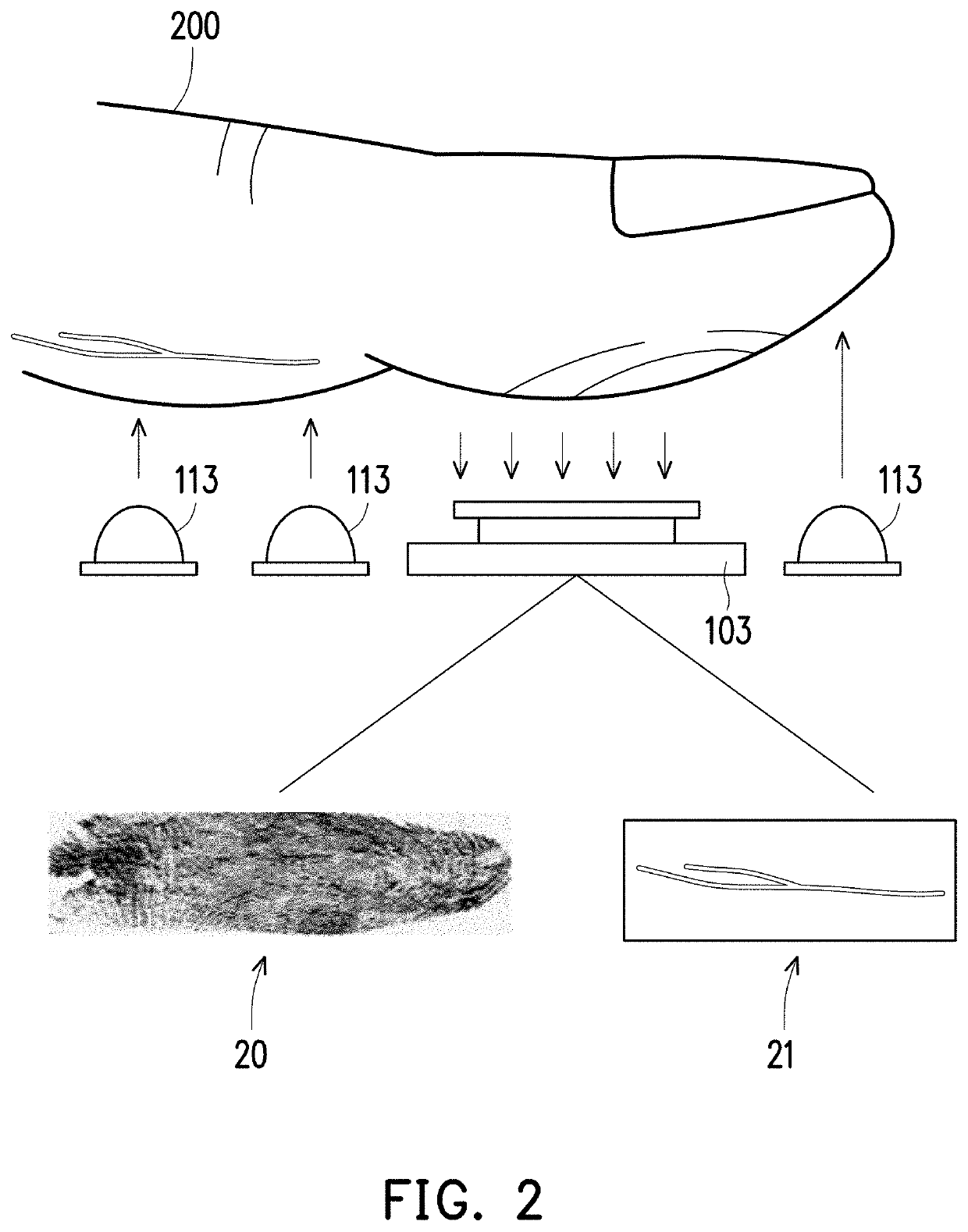
The invention is a device and method that can use multiple biological features, such as fingerprint and finger vein, for identification, improving accuracy and convenience. It uses an NIR optical principle to capture a finger image and an algorithm to obtain the optimal biological features for identification. This technology can be used for access control and attendance management of employees, and can also be used with other devices to create business opportunities in other fields such as finance industry and security industry.

Problems solved by technology

For example, some people have few fingerprint features, some people's fingerprints have worn down through long use and cannot be scanned into images, some people have skin peeling on their fingers, some people's fingers are dirty, the temperature of the environment is too low, etc., and the biggest risk is that it is easy to leave traces such that people with bad intentions may be able to copy a fingerprint onto a film and use it to fool an identification device.
However, a defect of finger vein identification is that a finger vein may change with age and physiology, and its permanence has not been confirmed.
Moreover, the equipment for acquiring a finger vein is not easy to miniaturize, a design thereof is relatively complex, and the manufacturing cost is high.

Method used


Image

  • Electronic device and method for obtaining features of biometrics
  • Electronic device and method for obtaining features of biometrics
  • Electronic device and method for obtaining features of biometrics

Examples


Embodiment Construction

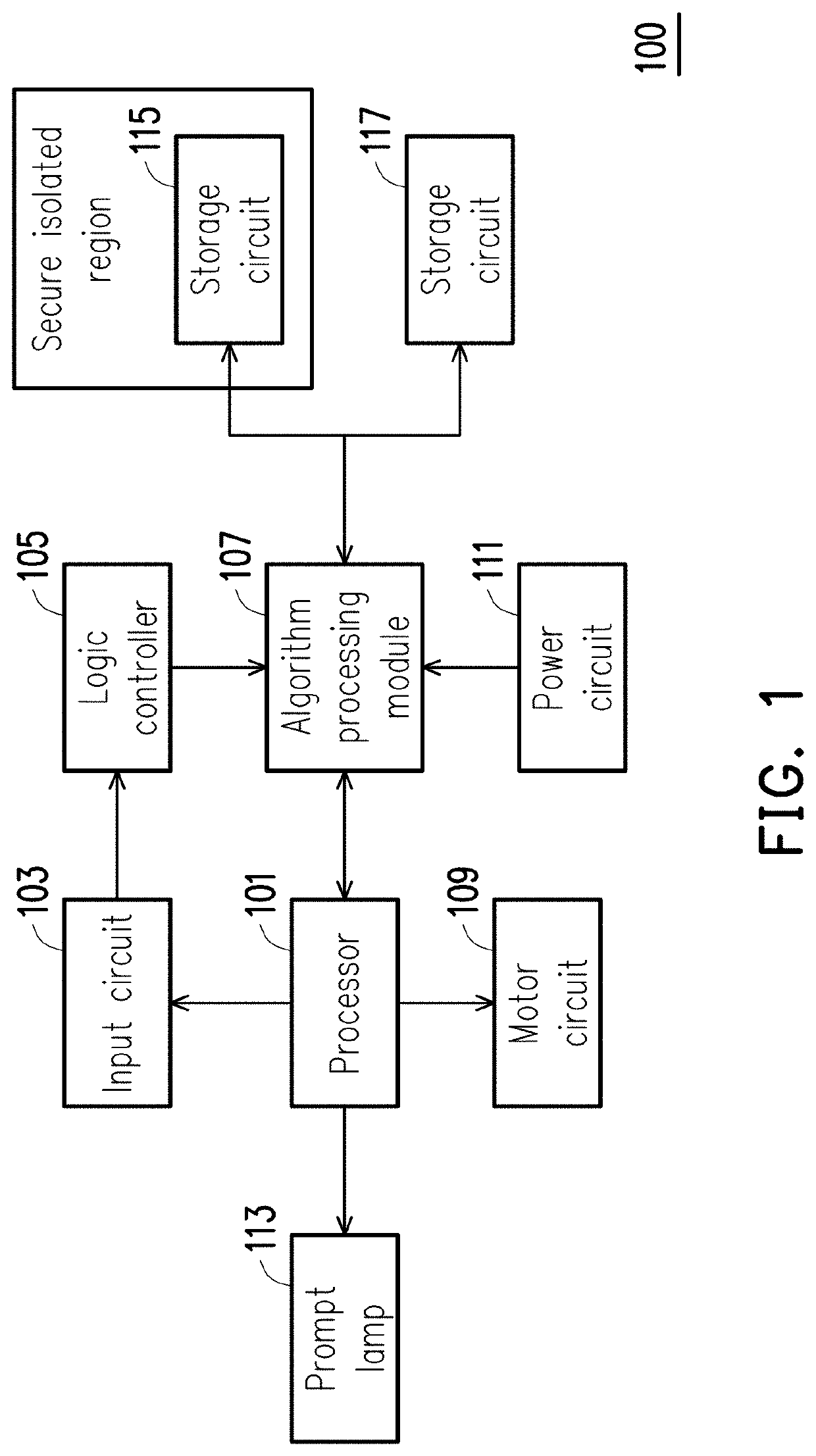
[0028]FIG. 1 is a schematic diagram of an electronic device according to an embodiment of the invention.

[0029]Referring to FIG. 1, an electronic device 100 includes a processor 101, an input circuit 103, a logic controller 105, an algorithm processing module 107, a motor circuit 109, a power circuit 111, a prompt lamp 113 and storage circuits 115 to 117.

[0030]The processor 101 may be a micro controller unit (MCU), or a processor integrating memory and computation functions of a central processing unit (CPU), a random-access memory (RAM), a read only memory (ROM) and an I / O device.

[0031]The input circuit 103 may include a finger sensor and an acquisition control circuit, and is configured to acquire a fingerprint image according to preset acquisition parameters, and transmit image data to the algorithm processing module 107.

[0032]The logic controller 105 may be a complex programmable logic device (CPLD), and is configured to access and pre-process the image acquired by the input circ...


PUM


Abstract

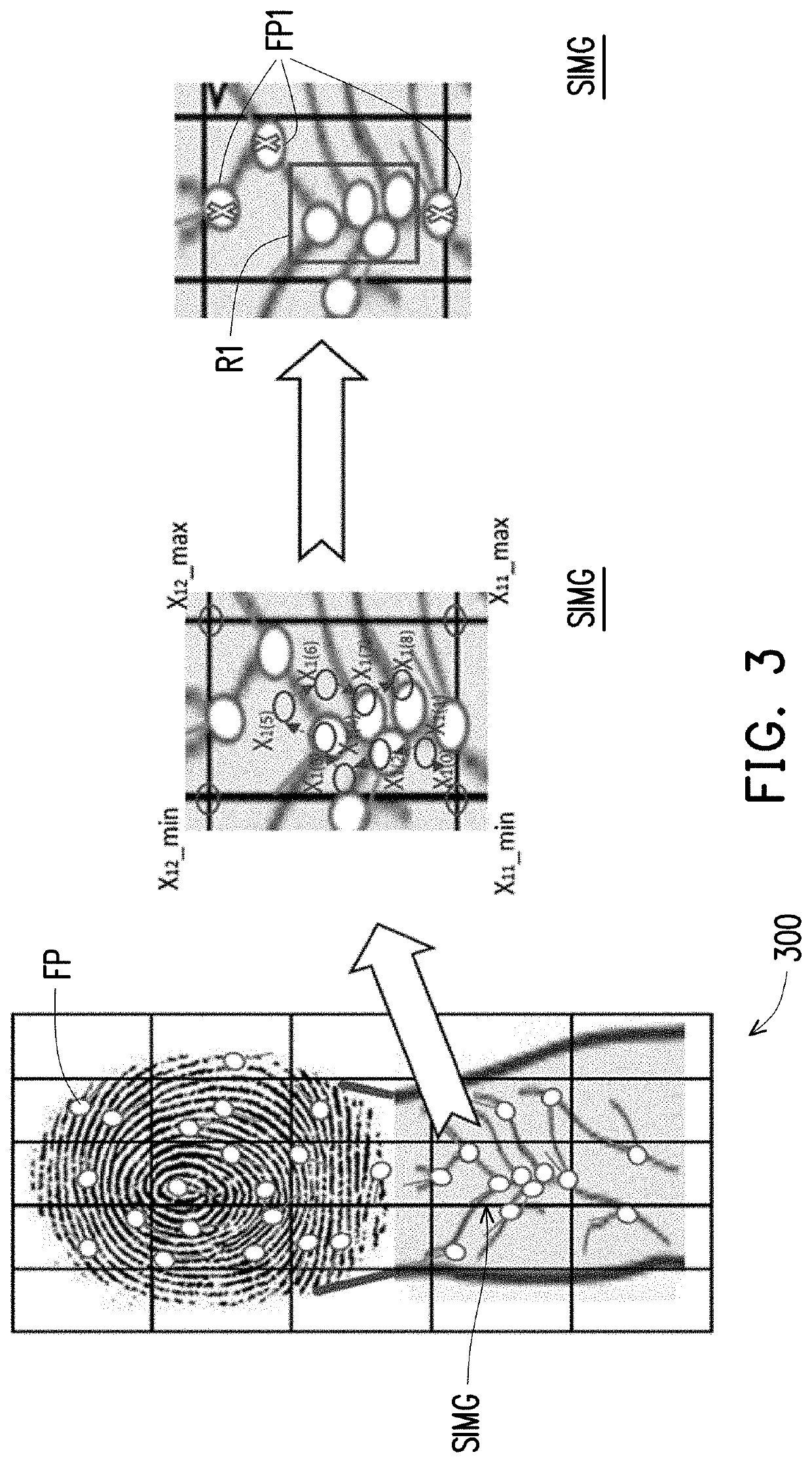
An electronic device and a method for obtaining features of biometrics are provided. The method includes: obtaining an image including a plurality of biological features; obtaining a plurality of feature points of the biological features in the image; dividing the image into a plurality of sub-images, and obtaining a region in each of the sub-images; and identifying from among a plurality of second feature points in the region in each of the sub-images a plurality of third feature points for performing a biometric operation.

Description

CROSS-REFERENCE TO RELATED APPLICATION[0001]This application claims the priority benefit of Taiwan application serial no. 108140599, filed on Nov. 8, 2019. The entirety of the above-mentioned patent application is hereby incorporated by reference herein and made a part of this specification.BACKGROUNDTechnical Field[0002]The invention relates to an electronic device and a feature obtaining method, and particularly relates to an electronic device and a method for obtaining features of biometrics.Description of Related Art[0003]Biometrics is a secure, reliable and accurate identity verification means using biological features that are usually unique, measurable, hereditary, or life-long, etc., with assistance of advanced computer technology nowadays, and can further realize applications such as automation, intelligent management, etc. At present, the most commonly used biometric techniques include fingerprint identification, human face identification, palmprint identification, voice (...

Claims


Application Information

Patent Timeline
Patent Type & Authority Applications(United States)
IPC IPC(8): G06K9/00G06F21/32H04L9/32
CPCG06K9/00067H04L9/3231G06F21/32G06K9/00087G06V40/1347G06V40/13G06V40/1365G06V40/12
Inventor LIAO, CHIEN-FU
Owner WISTRON CORP
Learn More