Multilayer structure and method for fabricating the same

Active Publication Date: 2021-05-13
MACRONIX INT CO LTD
View PDF0 Cites 0 Cited by
  • Summary
  • Abstract
  • Description
  • Claims
  • Application Information

AI Technical Summary

Benefits of technology

The invention describes a way to make a complicated and expensive multilayer structure by using a single process to create multiple conductive layers and connectors. This method simplifies the process and reduces costs.

Problems solved by technology

However, as the demand for the number of layers of the multilayer structure increases, the amount of conductive material required increases, and the process is more complicated, which may greatly increase the cost for fabricating.

Method used


Image

  • Multilayer structure and method for fabricating the same
  • Multilayer structure and method for fabricating the same
  • Multilayer structure and method for fabricating the same

Examples


Embodiment Construction

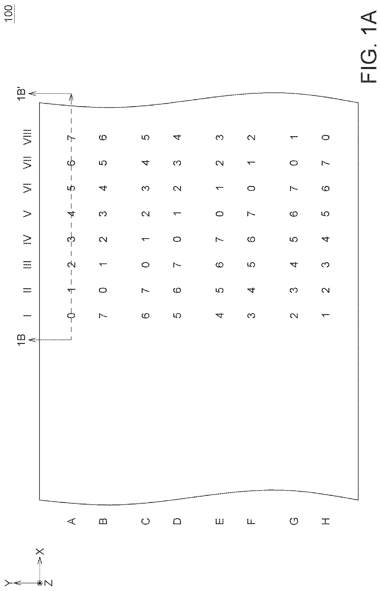
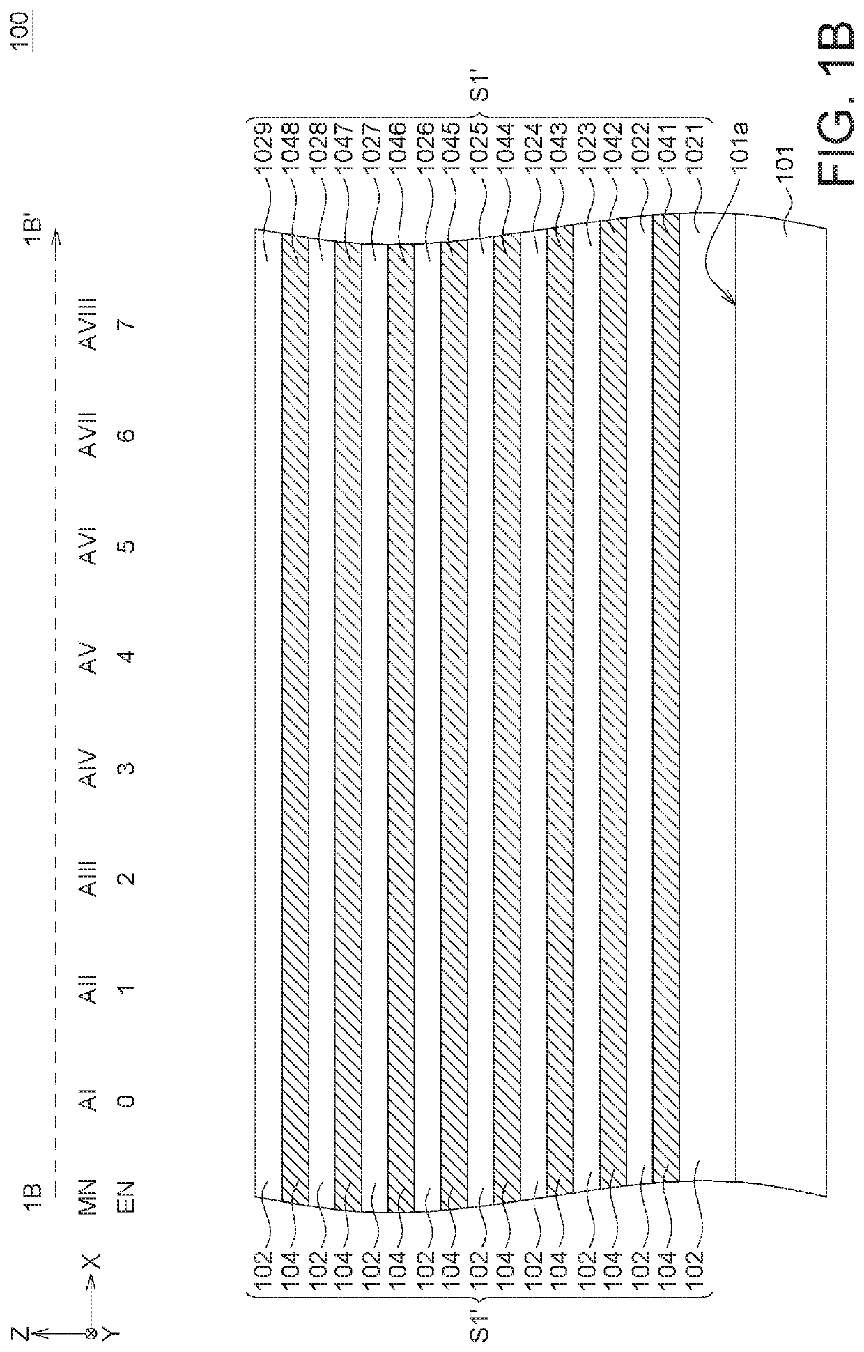
[0047]FIGS. 1A-25C are top views and cross-sectional views showing a method for fabricating a multilayer structure 100 in accordance with an embodiment of the present disclosure.

[0048]FIG. 1A is a top view of a method for fabricating a multilayer structure 100 in accordance with an embodiment of the present disclosure. FIG. 1B is a cross-sectional view taken along line 1B-1B′ of FIG. 1A.

[0049]Referring to FIGS. 1A and 1B simultaneously, a substrate 101 is provided, and a laminated body S1′ is formed on an upper surface 101a of the substrate 101. The laminated body S1′ includes a plurality of insulating layers 102 and a plurality of sacrificial layers 104 alternately stacked on the upper surface 101a of the substrate 101, for example, by a deposition process. In this embodiment, the insulating layer 102 has 9 layers, including the insulating layer 1021˜1029 from the bottom to the top layers, the sacrificial layer 104 has 8 layers, including the sacrificial layer 1041˜1048 from the bo...


PUM


Abstract

A multilayer structure includes a substrate and a plurality of sub-stacks extending along a first direction respectively and disposed on an upper surface of the substrate along a second direction. Each of the sub-stacks includes insulating layers and patterned sacrificial layers alternately stacked on the upper surface along a third direction; conductive layers alternately stacked on the upper surface with the insulating layers along the third direction; and interlayer connectors extending along the third direction; wherein the patterned sacrificial layers have first sides and second sides opposite to the first sides, the conductive layers include first side conductive layers corresponding to the first sides and second side conductive layers corresponding to the second sides; wherein the interlayer connectors are electrically connected and directly contact corresponding ones of the conductive layers, and the first direction, the second direction, and the third direction are crossed.

Description

BACKGROUND OF THE INVENTIONField of the Invention[0001]The invention relates in general to a multilayer structure and a method for fabricating the same, and more particularly to a multilayer structure used for a semiconductor device and a method for fabricating the same.Description of the Related Art[0002]The elements in a semiconductor device or between different semiconductor devices are generally electrically connected through interlayer connectors in a multilayer structure. In general, the multilayer structure includes a plurality of conductive layers and a plurality of insulating layers alternately stacked on a substrate, and the interlayer connectors formed of the conductive material extend in a vertical direction and are electrically connected to the specific conductive layer. However, as the demand for the number of layers of the multilayer structure increases, the amount of conductive material required increases, and the process is more complicated, which may greatly increa...

Claims


Application Information

Patent Timeline
IPC IPC(8): H01L23/498
CPCH01L23/49822H01L23/49838H01L23/49827H01L21/4853H01L21/76895H01L23/49811H01L23/528H01L23/5386H01L21/76816H01L21/76831H01L21/76838H01L23/5226H01L23/5383
Inventor CHEN, SHIH-HUNG
Owner MACRONIX INT CO LTD
Why Eureka
Try Eureka