Substrate and method for monitoring positions of boundaries of film layer on the substrate

a technology of substrate and film layer, which is applied in the direction of semiconductor devices, semiconductor/solid-state device details, instruments, etc., can solve the problems of reducing production efficiency, wasting a lot of debugging time, and reducing the accuracy of confirming the boundaries of film layers at the edges of display regions, so as to improve the accuracy of confirming the boundaries of film layers, shorten the start-up time, and increase production capacity

Active Publication Date: 2021-05-20
SHENZHEN CHINA STAR OPTOELECTRONICS TECH CO LTD
View PDF0 Cites 0 Cited by
  • Summary
  • Abstract
  • Description
  • Claims
  • Application Information

AI Technical Summary

Benefits of technology

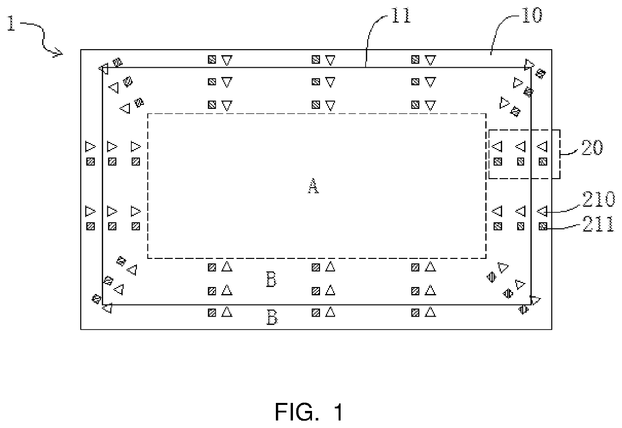
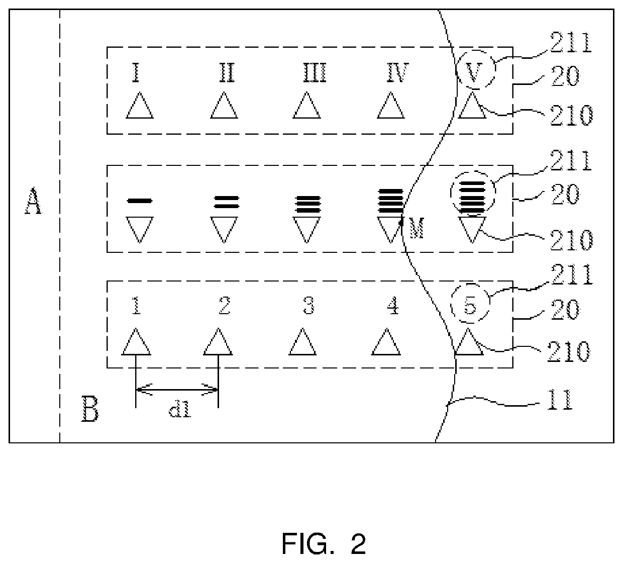
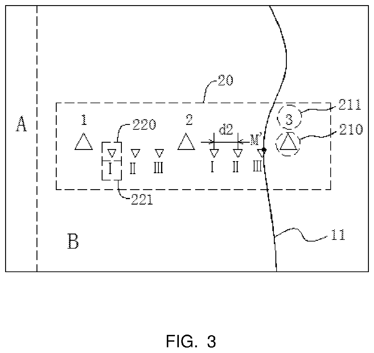
[0032]The beneficial effects of the claimed invention are: Compared with current method for monitoring positions of boundaries of a film layer disposed on a substrate, the present invention provides a plurality of sets of positioning units at positions corresponding to a non-display region around a substrate. Each set of positioning units is composed of a primary positioning mark and a corresponding primary positioning rule, and a secondary positioning mark and a secondary positioning rule nested under the primary positioning mark. With this design, an accuracy of confirming positions of boundaries of a film layer can be greatly improved, thereby shortening start-up time, increasing production capacity and reducing labor costs.

Problems solved by technology

Uniformity controls of the PI alignment films at edges of display regions have always been problems in TFT LCD processes.
Generally, offline manual measurements are adopted, which waste a lot of debugging time and reduce production efficiencies.
Therefore, current technologies have defects and urgently need improvements.

Method used


Image

  • Substrate and method for monitoring positions of boundaries of film layer on the substrate
  • Substrate and method for monitoring positions of boundaries of film layer on the substrate
  • Substrate and method for monitoring positions of boundaries of film layer on the substrate

Examples


Embodiment Construction

[0039]The technical solution in the embodiments of the present invention will be clearly and completely described below with reference to the accompanying drawings in the embodiments of the present invention. It is to be understood that the described embodiments are merely exemplary of the invention, and not restrictive of the full scope of the invention. All other embodiments, which can be obtained by a person skilled in the art without inventive step based on the embodiments of the present invention, are within the scope of the present invention.

[0040]In the description of the present invention, it is to be understood that the terms “center,”“longitudinal,”“lateral,”“length,”“width,”“thickness,”“upper,”“lower,”“front,”“rear,”“left,”“right,”“vertical,”“horizontal,”“top,”“bottom,”“inner,”“outer,”“clockwise,”“counterclockwise,” and the like are used in the orientations and positional relationships indicated in the drawings for convenience in describing the present invention and for s...


PUM

PropertyMeasurementUnit
distanceaaaaaaaaaa
distanceaaaaaaaaaa
thicknessaaaaaaaaaa

Abstract

The present invention provides a substrate and a method for monitoring positions of boundaries of a film layer disposed on a substrate. A plurality of sets of positioning units are provided in a non-display region of the substrate. Each set of the positioning units includes at least two primary positioning marks and corresponding primary positioning rulers. There are at least two secondary positioning marks and corresponding secondary positioning rulers disposed between the two adjacent primary positioning marks. The present invention determines a specific position of the boundaries of the film layer according to readings of the positioning rulers of the plurality of sets of positioning units corresponding to the boundaries of the film layer.

Description

[0001]This application claims filed Nov. 19, 2019 Chinese Patent Application No. 201911131299.3, entitled “Substrate and method for monitoring positions of boundaries of film layer on the substrate” in Chinese Priority Patent Application, the entire content of which is incorporated by reference in the present application.FIELD OF INVENTION[0002]The present application relates to the field of productions of liquid crystal displays, and in particular, to a substrate and a method for monitoring positions of boundaries of a film layer disposed on a substrate.BACKGROUND OF INVENTION[0003]Generally, alignment films of TFT LCDs are polyimide films (that is, PI alignment films), which allow liquid crystals to be neatly arranged in liquid crystal cells through physical or chemical action to form ordered pretilt angles so that the LCDs can display normally. A uniformity of a thickness of the PI alignment films is directly related to an alignment ability of the PI alignment films. Uniformity c...

Claims


Application Information

Patent Timeline
Patent Type & Authority Applications(United States)
IPC IPC(8): H01L23/544G02F1/1337
CPCH01L23/544H01L2223/54426G02F1/1337G02F1/133374
Inventor YU, YUNLU, HUAJUNYAN, YUE
Owner SHENZHEN CHINA STAR OPTOELECTRONICS TECH CO LTD
Why Eureka
Try Eureka