Method for driving semiconductor device

a technology of semiconductor devices and driving parts, applied in the direction of power consumption reduction, pulse techniques, instruments, etc., can solve the problems of increasing power consumption in standby state, and achieve the effects of reducing power consumption, reducing starting time, and preventing power supply

Active Publication Date: 2013-11-28
SEMICON ENERGY LAB CO LTD
View PDF11 Cites 41 Cited by
  • Summary
  • Abstract
  • Description
  • Claims
  • Application Information

AI Technical Summary

Benefits of technology

[0022]The potentials of the first node and the second node can be held during a period which is necessary (from 10 milliseconds to 10 years) in such a manner that a transistor whose channel region is formed in a wide-gap semiconductor is formed as each of the first transistor and the second transistor connected to the first node and the second node, respectively, and the capacitance of the first capacitor and the capacitance of the second capacitor are set or selected appropriately. Therefore, it is possible to stop supply of power to the semiconductor device when not used; accordingly, power consumption can be reduced. Moreover, it is not necessary to rewrite data to the first node and the second node at the start-up of the semiconductor device; thus, the starting time can be shortened and the power consumption can be reduced.
[0023]Further, after the first potential is held in the first node to which the one of the source and the drain of the first transistor, the one of the pair of electrodes of the first capacitor, and the gate of the third transistor are connected or the second node to which the one of the source and the drain of the second transistor, the one of the pair of electrodes of the second capacitor, and the gate of the fourth transistor are connected, the second potential higher than the first potential is held in the first node or the second node, whereby characteristics higher than or equal to those of a transmission gate can be obtained. Accordingly, a p-channel transistor is not necessary and it is possible to reduce the area of the selection circuit.
[0024]Furthermore, the gate of the third transistor or the gate of the fourth transistor is supplied with a potential which can turn on the third transistor or the fourth transistor regardless of the potentials of the signals input into the first input terminal and the second input terminal. In one embodiment of the present invention, even without a circuit such as an SRAM, which includes an inverter, it is possible to turn on or off the transistors T3 or T4; therefore, standby current does not flow and power consumption can be reduced greatly.
[0025]According to one embodiment of the present invention, it is possible to reduce power consumption of a semiconductor device including a selection circuit, reduce the area of the selection circuit in the semiconductor device, and downsize the size of the semiconductor device.

Problems solved by technology

The standby current increases significantly with miniaturization of a circuit; therefore, an increase in power consumption in a standby state has been a problem.

Method used


Image

  • Method for driving semiconductor device
  • Method for driving semiconductor device
  • Method for driving semiconductor device

Examples


embodiment 1

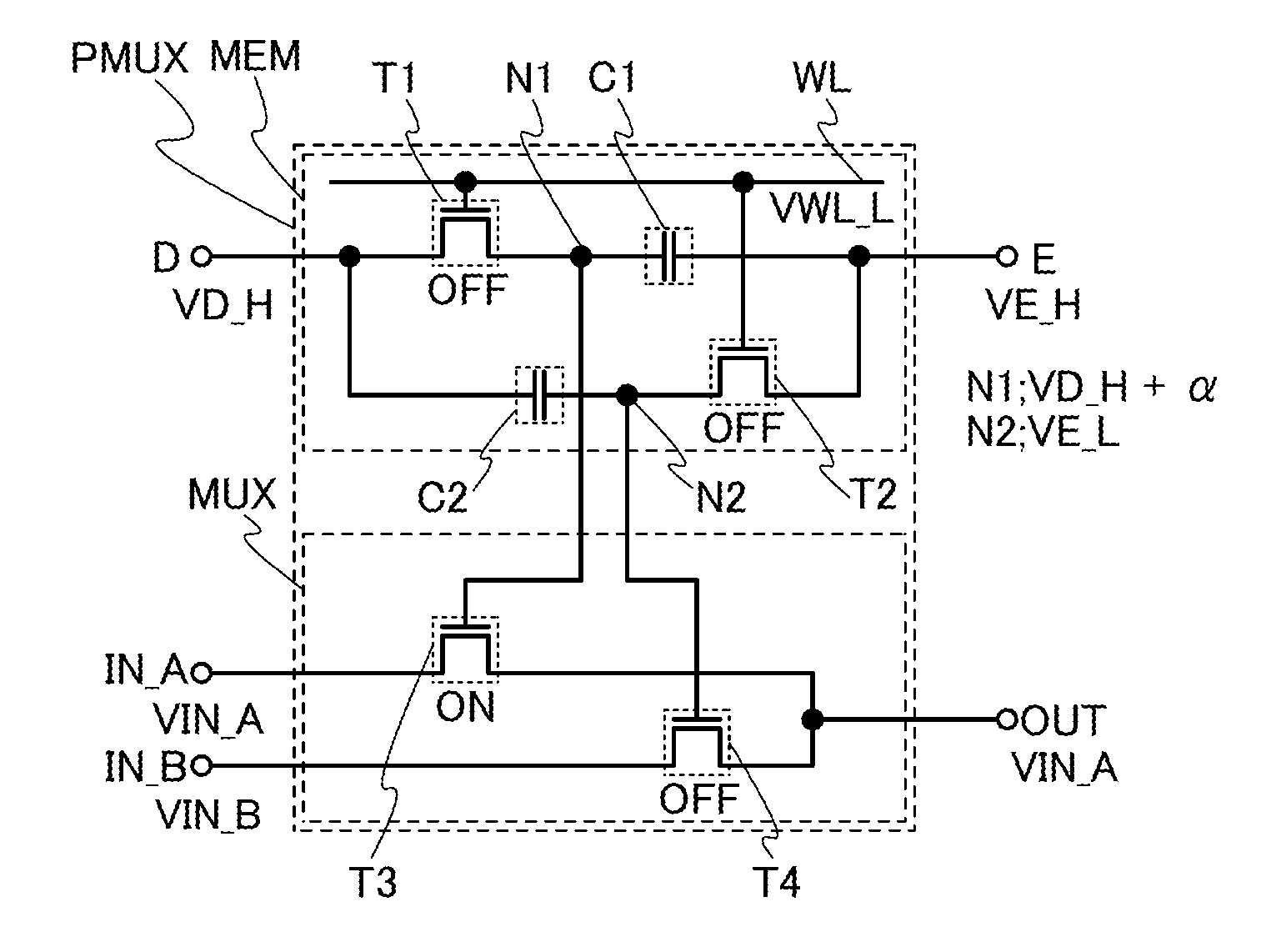
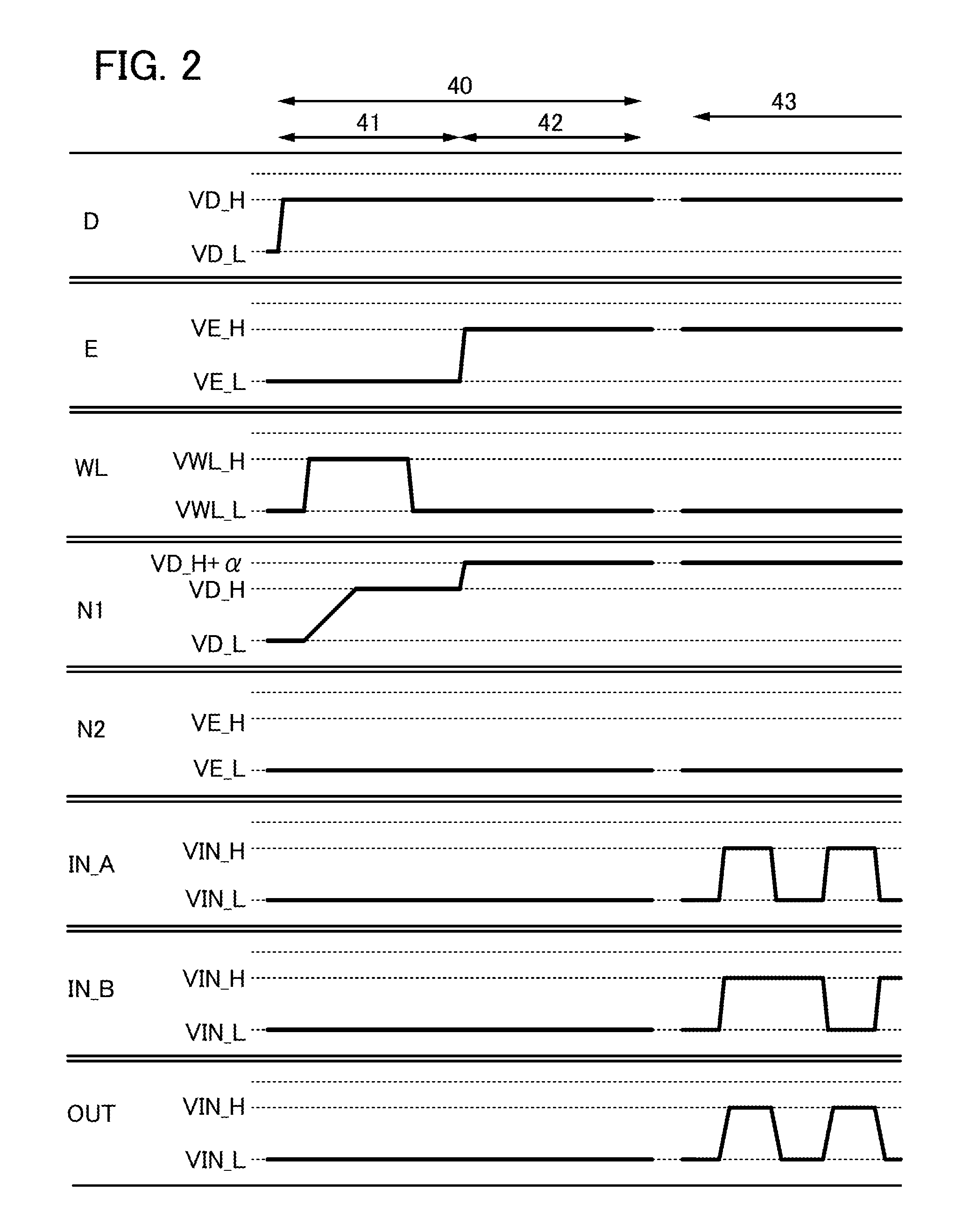
[0043]In this embodiment, one embodiment of a semiconductor device including a selection circuit and a method for driving the semiconductor device will be described with reference to FIG. 1, FIG. 2, FIGS. 3A and 3B, and FIG. 4.

[0044]FIG. 1 is a circuit diagram of a selection circuit PMUX including a memory MEM and a multiplexer MUX.

[0045]In FIG. 1, the memory MEM includes a transistor T1, a capacitor C1, a transistor T2, and a capacitor C2.

[0046]In the transistor T1, one of a source and a drain is connected to a terminal D, the other of the source and the drain is connected to a first electrode of the capacitor C1, and a gate is connected to a word line WL. A second electrode of the capacitor C1 is connected to a terminal E.

[0047]In the transistor T2, one of a source and a drain is connected to the terminal E, the other of the source and the drain is connected to a first electrode of the capacitor C2, and a gate is connected to the word line WL. A second electrode of the capacitor C...

embodiment 2

[0083]In this embodiment, a semiconductor device including the selection circuit described in Embodiment 1 will be described. Note that here, the semiconductor device includes, in its category, a variety of semiconductor integrated circuits formed using semiconductor elements, such as memory devices, processors, central processing units (CPUs), image processing circuits, digital signal processors (DSPs), microcontrollers, and reconfigurable logic circuits. In addition, the semiconductor device of the present invention also includes, in its category, various devices formed using the above semiconductor integrated circuits, such as RF tags and display devices. The display devices include, in its category, liquid crystal display devices, light-emitting devices having pixels each provided with a light-emitting element typified by an organic light-emitting element (OLED), electronic paper, digital micromirror devices (DMDs), plasma display panels (PDPs), field emission displays (FEDs), a...

embodiment 3

[0100]In this embodiment, a structure of the selection circuit will be described with reference to FIGS. 8A and 8B, FIGS. 9A and 9B, and FIGS. 10A and 10B.

[0101]FIGS. 8A and 8B and FIGS. 9A and 9B are plan views illustrating the positions and shapes of main structures in the multiplexer and the memory of the selection circuit. FIG. 10A is a cross-sectional view taken along dot-dash-line A-B in FIGS. 8A and 8B and FIGS. 9A and 9B, and FIG. 10B is a cross-sectional view taken along dot-dash-line C-D in FIGS. 8A and 8B and FIGS. 9A and 9B. Note that in FIGS. 10A and 10B, a transistor 704a and a transistor 704b correspond to the transistor T3 and the transistor T4 shown in FIG. 1, respectively, and a transistor 750 corresponds to the transistor T1 shown in FIG. 1. Further, a capacitor 751 corresponds to the capacitor C1 shown in FIG. 1.

[0102]The transistors 704a and 704b are n-channel transistor (NMOSFET). The transistors 704a and 704b are electrically isolated from other elements by a ...


PUM


Abstract

A method for driving a semiconductor device capable of reducing an area of a multiplexer and reducing its power consumption is provided. In a method for operating a semiconductor device including a memory and a multiplexer, a first transistor is connected to a first capacitor, and a second transistor is connected to a second capacitor. In the multiplexer, in a third transistor, a source is connected to a first input terminal and a drain is connected to an output terminal and, in a fourth transistor, a source is connected to a second input terminal and a drain is connected to the output terminal. Further, a step of holding a first potential in a node to which the first transistor, the first capacitor, and a gate of the third transistor are connected and holding a second potential higher than the first potential in the node is included.

Description

BACKGROUND OF THE INVENTION[0001]1. Field of the Invention[0002]The present invention relates to a method for driving a semiconductor device including a selection circuit and an electronic device including the semiconductor device.[0003]2. Description of the Related Art[0004]In an integrated circuit, a multiplexer is used as a selection circuit for selecting an input signal, for example. The multiplexer is a circuit for outputting one output signal from a plurality of input signals. Here, a reconfigurable logic circuit is described as an example of a semiconductor device including multiplexers.[0005]The reconfigurable logic circuit includes a plurality of logic blocks each including a plurality of logic elements, a plurality of wirings for connecting the logic blocks, a programmable switch, and an input / output block.[0006]The reconfigurable logic circuit can have a logical structure with a high degree of flexibility by changing the function of each logic element or connecting the lo...

Claims


Application Information

Patent Timeline
Patent Type & Authority Applications(United States)
IPC IPC(8): H03K19/00
CPCH03K19/0013H03K19/1737H03K19/1776H10B10/12G11C11/412
Inventor TAKEMURA, YASUHIKO
Owner SEMICON ENERGY LAB CO LTD
Why Eureka
Try Eureka