Semiconductor device

a semiconductor and register technology, applied in the field of shift registers, can solve the problems of large power consumption, large power consumption, complex circuit shown in fig. 19 where the nor circuit b>1903/b> is provided, and achieve the effect of reducing cost and siz

Active Publication Date: 2005-11-24
SEMICON ENERGY LAB CO LTD
View PDF5 Cites 20 Cited by
  • Summary
  • Abstract
  • Description
  • Claims
  • Application Information

AI Technical Summary

Benefits of technology

[0025] In this manner, according to the invention, reduction in cost and size can be realized, and a circuit can operate normally in more cases.

Problems solved by technology

However, the clock signal is supplied to all unit registers constituting the shift register, so that a large load is applied to a wiring for supplying the clock signal, which results in large power consumption.
Consequently, a large load is applied to a wiring for supplying the clock signal, which results in large power consumption.
Furthermore, the circuit shown in FIG. 19 where the NOR circuit 1903 is provided is complex.
Accordingly, a transistor to turn OFF is not turned OFF, which leads to malfunction.
In addition, current continues to flow in the transistor which is not turned OFF, so that power consumption is increased.

Method used


Image

  • Semiconductor device
  • Semiconductor device
  • Semiconductor device

Examples


embodiment mode 1

[0049] Although the invention will be described by way of Embodiment Modes with reference to the accompanying drawings, it is to be understood that various changes and modifications will be apparent to those skilled in the art. Therefore, unless such changes and modifications depart from the scope of the invention, they should be construed as being included therein. It is to be noted that the same portion is denoted by the same reference numeral in different drawings in the structure of the invention described below.

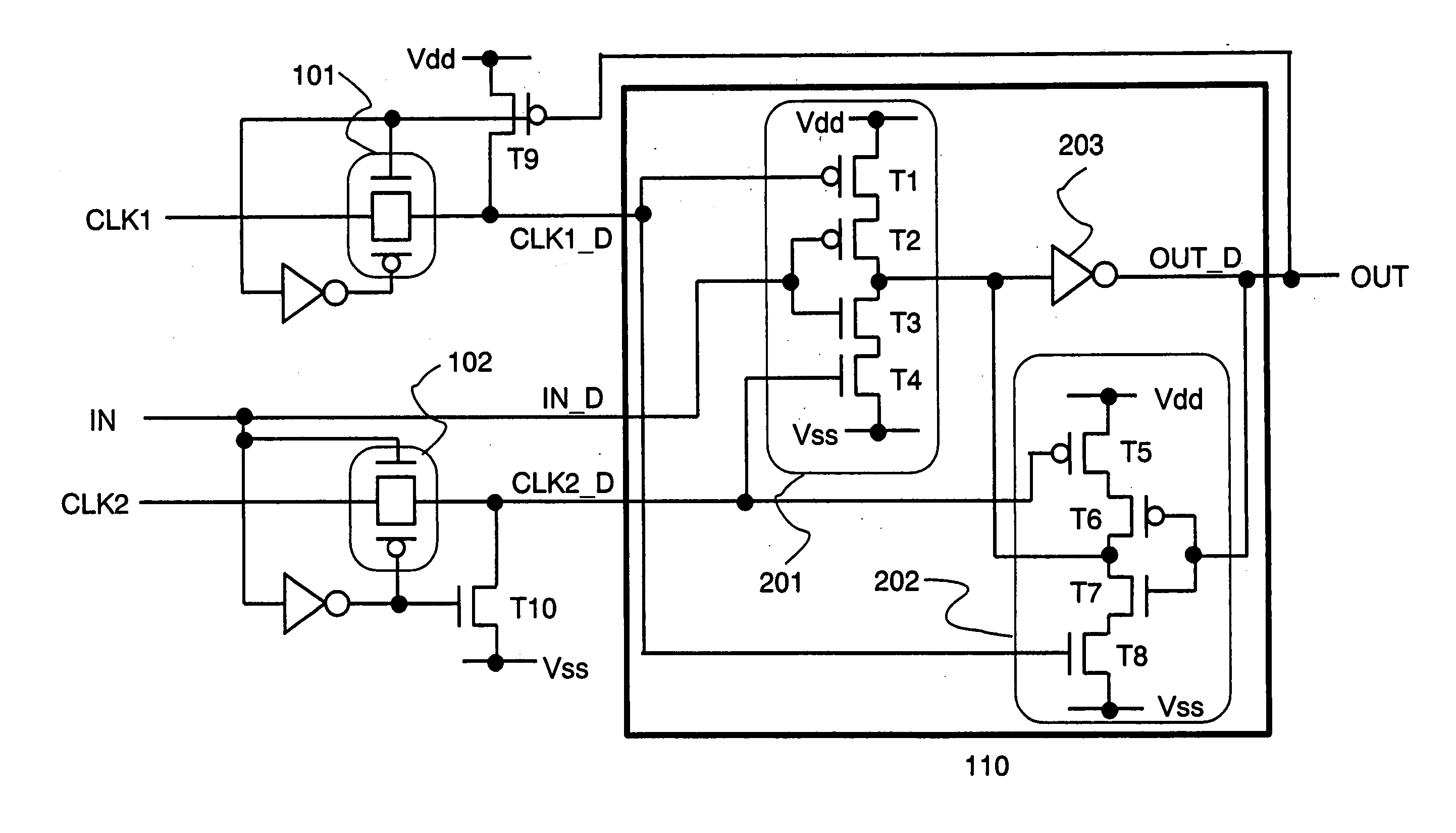
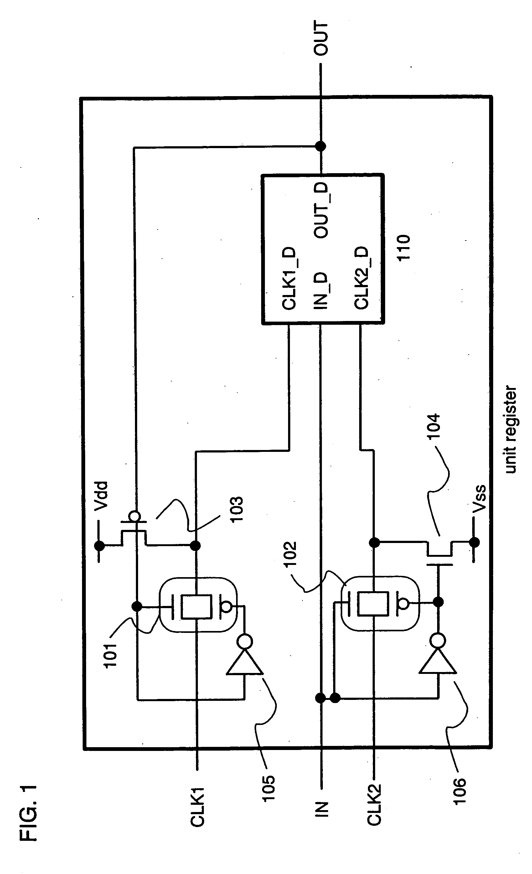
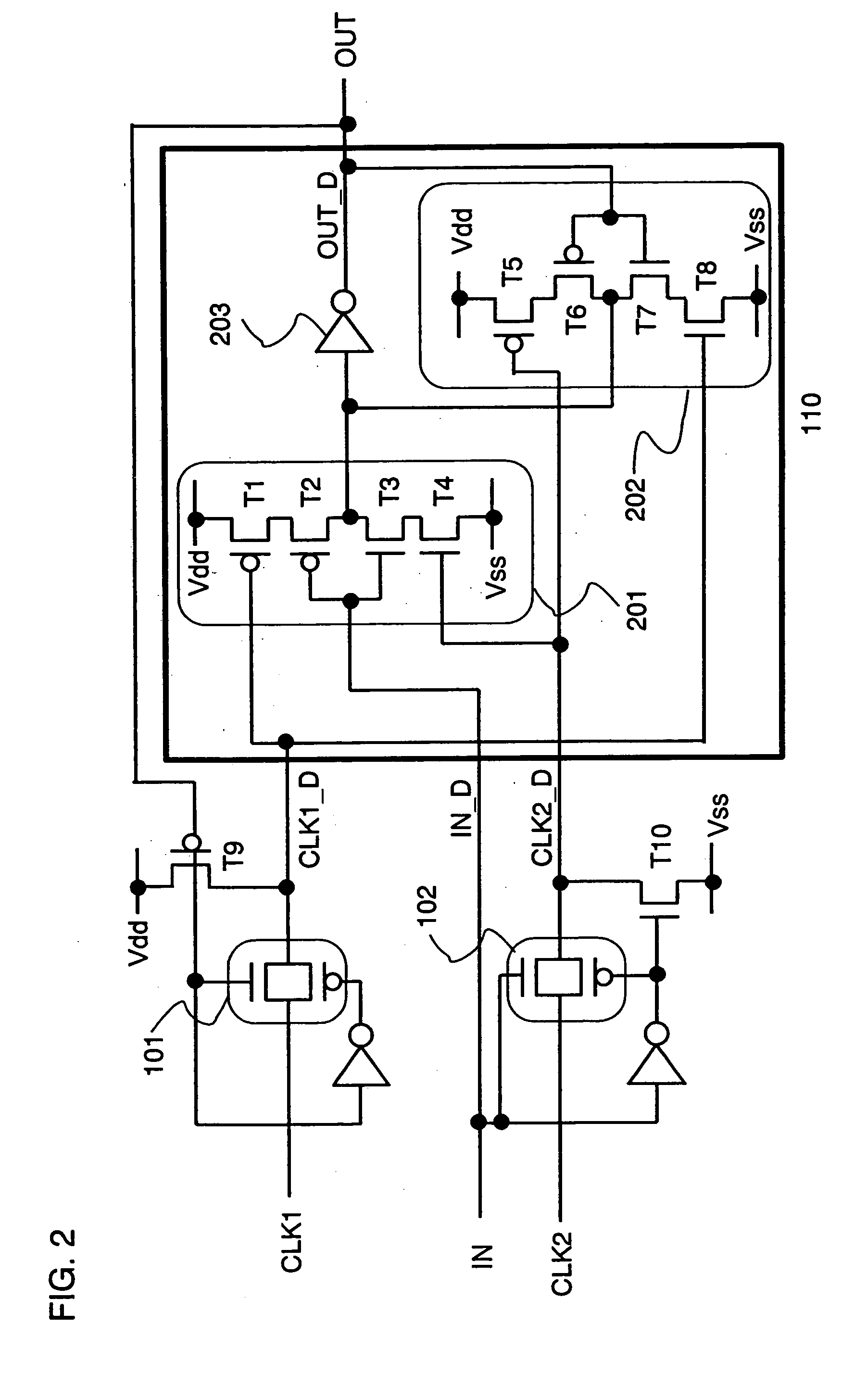
[0050]FIG. 1 shows exemplary constitution of one stage of a shift register. It is to be noted here that one or several stages of a shift register are called a unit register. A unit register is constituted by switches 101 and 102, transistors 103 and 104, inverters 105 and 106, and a flip-flop circuit 110. One of gate electrodes of the switch 101 is connected to a gate electrode of the transistor 103 and the input side of the inverter 105, while the other is connected to...

embodiment mode 2

[0078] In this embodiment mode, constitution of a display device, a signal line driver circuit, a gate line driver circuit, or the like, and operation thereof are described. A circuit of the invention can be employed partially to the signal line driver circuit and the gate line driver circuit.

[0079] A display device comprises a pixel array 1601, a gate line driver circuit 1602, and a signal line driver circuit 1610 as shown in FIG. 16. The gate line driver circuit 1602 outputs a selection signal sequentially to the pixel array 1601. The gate line driver circuit 1602 is constituted by a shift register 1621, a buffer circuit 1622, and the like.

[0080] Here, the circuit described in Embodiment Mode 1 which is shown in FIGS. 1 to 3 and FIGS. 11 to 15 for example is employed to the shift register 1621. Accordingly, the load on a wiring for supplying a clock signal is reduced and the dullness of the waveform of the clock signal is suppressed, which leads to normal operation of a circuit....

embodiment mode 3

[0099] Described in this embodiment mode with reference to FIGS. 22A and 22B is a structure of a display panel comprising the shift register described in Embodiment Mode 1.

[0100]FIG. 22A is a top view of a display panel and FIG. 22B is a cross-sectional view of FIG. 22A taken along a line A-A′. A signal line driver circuit 2001, a pixel portion 2002, and a scan line driver circuit 2006 are included, which are shown by a dotted line. In addition, a sealing substrate 2004, a sealant 2005, and a space 2007 surrounded by the sealant 2005 are included. The shift register of the invention is provided in the signal line driver circuit 2001 and the scan line driver circuit 2006.

[0101] A wiring 2008 is for transmitting signals to be inputted to the scan line driver circuit 2006 and the signal line driver circuit 2001, and receives a video signal, a clock signal, a start signal, and the like from an FPC (Flexible Printed Circuit) 2009. An IC chip (a semiconductor chip provided with a memory...


PUM


Abstract

A shift register capable of supplying only a necessary clock signal to a necessary unit register with simple constitution. A semiconductor device is provided with a shift register in which a plurality of stages of unit registers is connected, in which the unit register comprises a flip-flop circuit, a first switch and a second switch, a first clock signal line is electrically connected to the flip-flop circuit through the first switch, a second clock signal line is electrically connected to the flip-flop circuit through the second switch, the first switch is controlled to be on/off by an output signal from the flip-flop circuit, and the second switch is controlled to be on/off by an input signal to the flip-flop circuit.

Description

BACKGROUND OF THE INVENTION [0001] 1. Field of the Invention [0002] The present invention relates to a shift register employing a transistor, and particularly, relates to a shift register for controlling a display device. [0003] 2. Description of the Related Art [0004] In display devices employing light emitting elements of a self-luminous type typified by an organic light emitting diode (OLED which is also called an organic EL element, an electroluminescence element, or the like) and liquid crystal display devices, a circuit for driving pixels is formed over the same substrate as the pixels. In such a circuit, a signal to sequentially select a plurality of wirings, a plurality of circuits (e.g., switches), or the like is required to be generated, therefore, a shift register is employed in many cases. [0005] A shift register is generally supplied with clock signals, and operates in synchronization with the clock signals. However, the clock signal is supplied to all unit registers co...

Claims


Application Information

Patent Timeline
Patent Type & Authority Applications(United States)
IPC IPC(8): G09G3/20G09G3/32G11C19/00G11C19/28
CPCG09G3/20G09G3/3208G09G2300/08G11C19/28G09G2310/0275G11C19/00G09G2310/0267
Inventor KIMURA, HAJIME
Owner SEMICON ENERGY LAB CO LTD
Why Eureka
Try Eureka