Metal filling under m1 layer of semiconductor devices
- Summary
- Abstract
- Description
- Claims
- Application Information
AI Technical Summary
Benefits of technology
Problems solved by technology
Method used
Image

Examples
Embodiment Construction
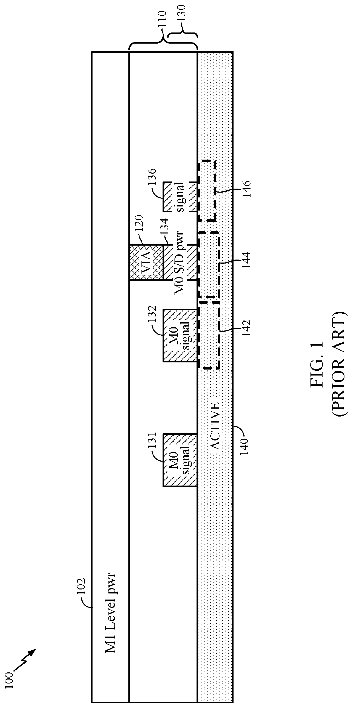
” one will understand how the features of this disclosure provide advantages that include decreased resistance of PDNs in semiconductor devices, improved integrated circuit (IC) reliability, and simplified metal layer 3 (M3) patterning in IC fabrication processes.
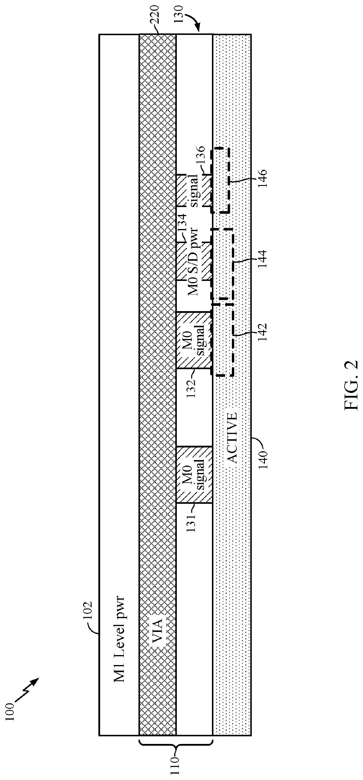
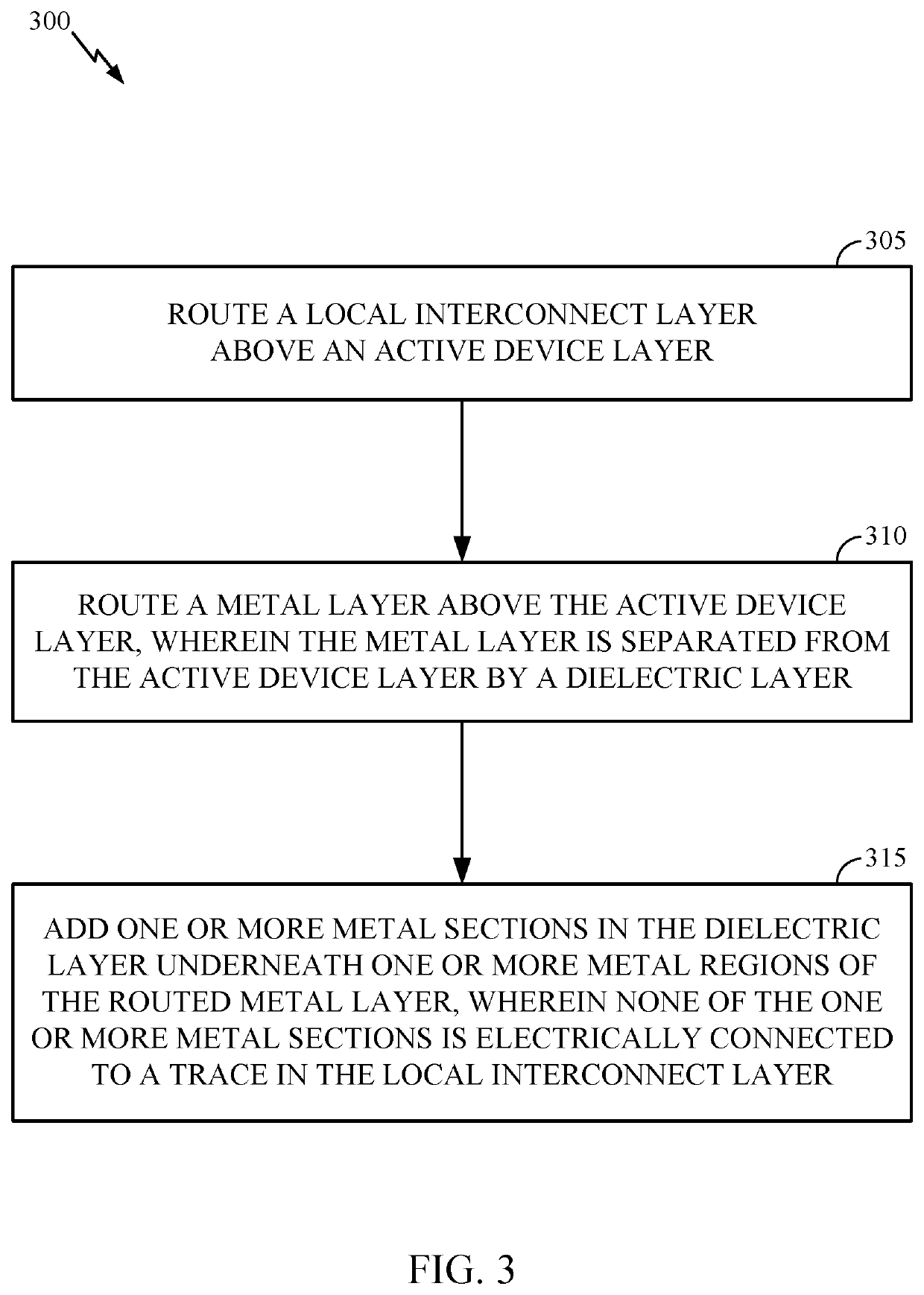
[0007]Certain aspects of the present disclosure provide a method for fabricating a semiconductor device. The method generally includes routing a local interconnect layer above an active device layer; routing a metal layer above the active device layer, wherein the metal layer is separated from the active device layer by a dielectric layer; and adding one or more metal sections in the dielectric layer underneath one or more metal regions of the routed metal layer, wherein none of the one or more metal sections is electrically connected to a trace in the local interconnect layer.
[0008]Certain aspects of the present disclosure provide a semiconductor device. The semiconductor device generally includes an active device layer; a...
PUM
 Abstract
Description
Claims
Application Information
 - Generate Ideas
- Intellectual Property
- Life Sciences
- Materials
- Tech Scout
- Unparalleled Data Quality
- Higher Quality Content
- 60% Fewer Hallucinations
Browse by: Latest US Patents, China's latest patents, Technical Efficacy Thesaurus, Application Domain, Technology Topic, Popular Technical Reports.
© 2025 PatSnap. All rights reserved.Legal|Privacy policy|Modern Slavery Act Transparency Statement|Sitemap|About US| Contact US: help@patsnap.com