

Biosensor with porous wicking layer
- Summary
- Abstract
- Description
- Claims
- Application Information
AI Technical Summary
Benefits of technology
Problems solved by technology
Method used
Image

Examples
example
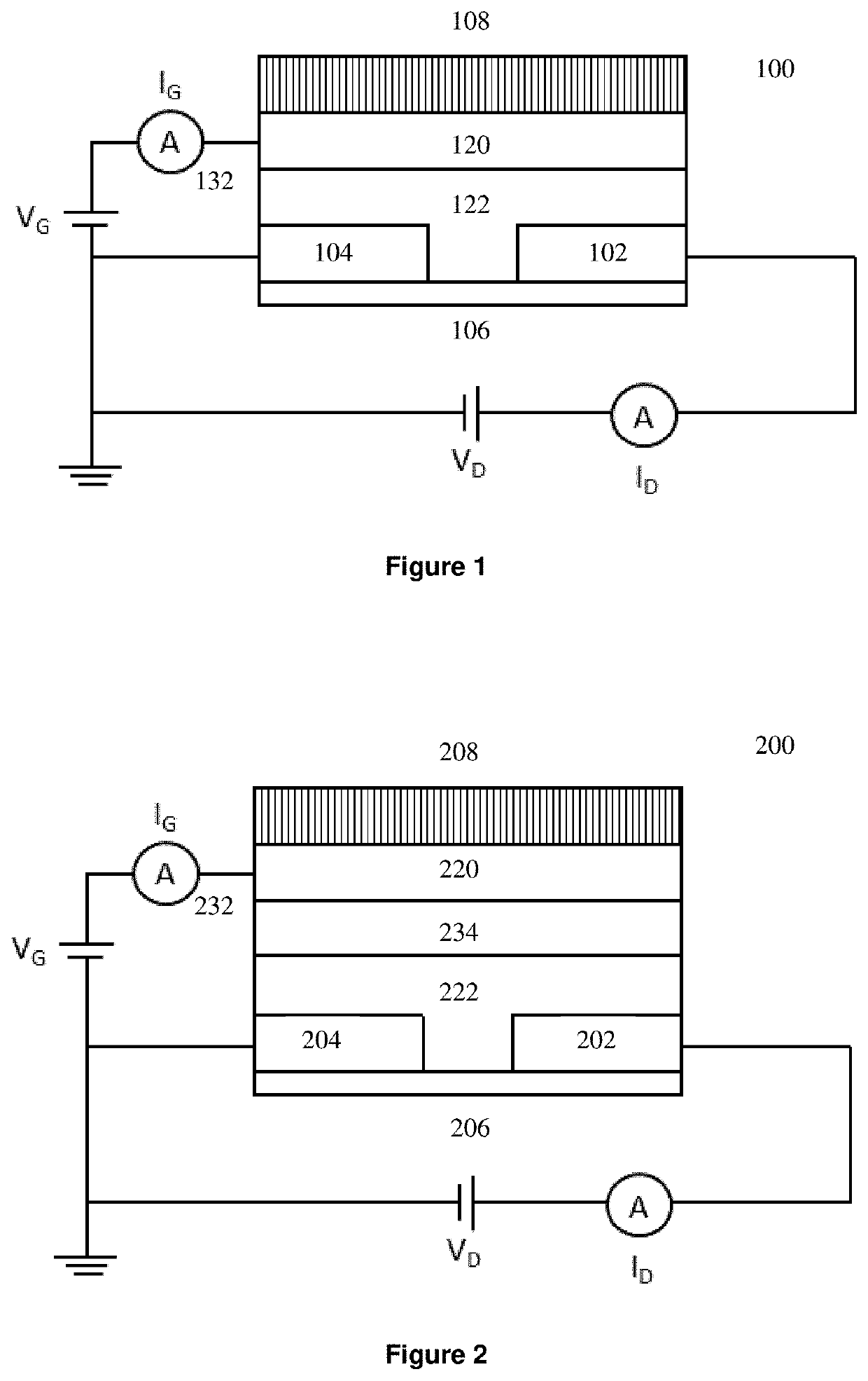
[0074]Fabrication of the Device
[0075]Pre-patterned ITO-on-glass substrates (15 Ω□−1 ITO, Xin Yan Technology) were used as the substrate and electrodes of the devices. Poly-3-hexylthiophene (P3HT) (MW ˜20 000) was dissolved in CHCl3 (Sigma-Aldrich) at various concentrations and sonicated for ˜1 hour or until the material was entirely dissolved. Poly-4-vinylphenol (PVP) (Sigma-Aldrich) was dissolved in ethanol (Sigma-Aldrich) at a concentration of 80 mg mL−1 and sonicated for ˜1 hour or until the material was entirely dissolved. Nafion solution (5% by weight in lower aliphatic alcohols and water, Sigma-Aldrich) was used as received.
[0076]The pre-patterned ITO-on-glass substrates were cleaned with methanol and purified water. P3HT solution in CHCl3 was spin-coated onto the substrates at 2000 rpm for 60 seconds. P3HT solutions of 5 mg mL−1, 10 mg mL−1, 15 mg mL−1, 20 mg mL−1, and 40 mg mL−1 were prepared, with average thicknesses of films spun from these concentrations of P3HT were 22 n...
PUM
| Property | Measurement | Unit |
|---|---|---|
| Fraction | aaaaa | aaaaa |
| Fraction | aaaaa | aaaaa |
| Pore size | aaaaa | aaaaa |
Abstract
Description
Claims
Application Information