
Multilayer ceramic electronic component

Active Publication Date: 2021-07-29
MURATA MFG CO LTD
View PDF0 Cites 1 Cited by
  • Summary
  • Abstract
  • Description
  • Claims
  • Application Information

AI Technical Summary

Benefits of technology

This patent describes a feature that allows for the creation of ceramic electronic components that can withstand direct external impact. The result is a stronger, more durable component that can withstand damage and maintain its performance.

Problems solved by technology

Unfortunately, the structure disclosed in Japanese Unexamined Patent Application, Publication No. 2012-44149 does not have sufficient strength because the surface of the element remains ceramic, in which defects, such as microcracks, exist as potential fracture starting points.

Method used


Image

  • Multilayer ceramic electronic component
  • Multilayer ceramic electronic component
  • Multilayer ceramic electronic component

Examples


first modification

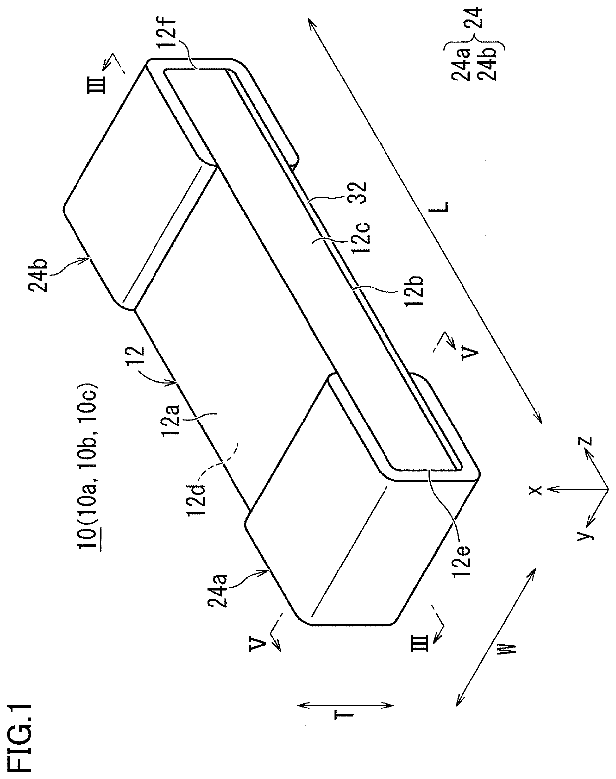
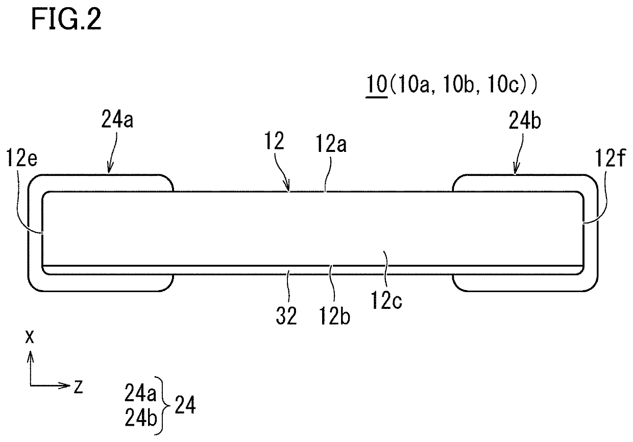
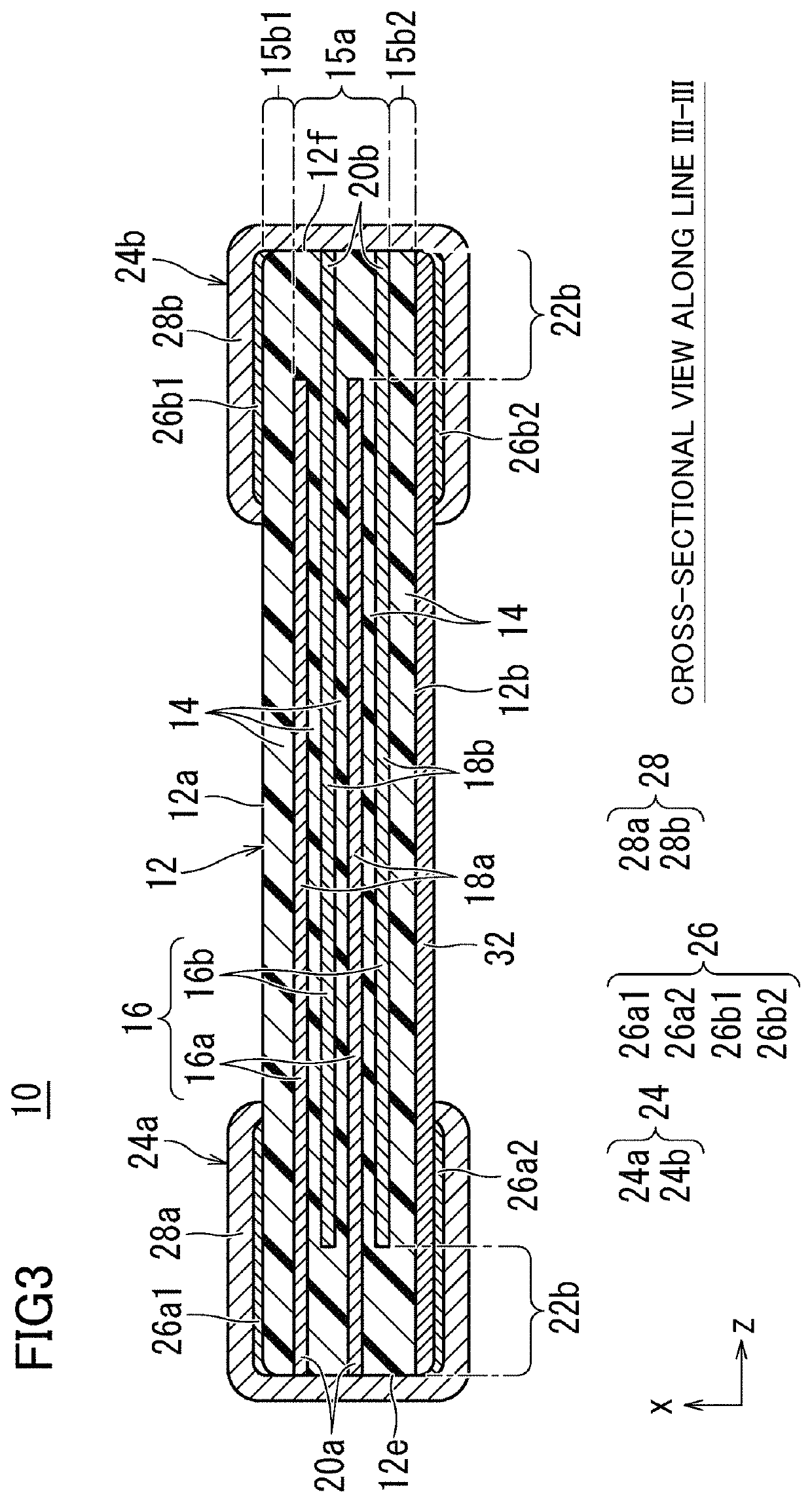
[0120]A multilayer ceramic capacitor 110 as a multilayer ceramic electronic component according to a first modification of the above-described preferred embodiment will be described below. As shown in FIG. 6, the multilayer ceramic capacitor 110 according to the first modification includes protective layers 32 and 34 disposed on the first main surface 12a and the second main surface 12b.

[0121]Accordingly, in the first modification, the protective layer 34 is further provided on the first main surface 12a, while the protective layer 32 is provided only on the second main surface 12b in the above-described preferred embodiment. In other words, the multilayer body 12 is sandwiched between upper and lower DLC layers.

[0122]This feature improves the mechanical strength of the center of both surfaces of the multilayer body 12 and the ends of the external electrodes 24 in the chip, namely, the multilayer ceramic capacitor. This is effective in improving the resistance to thermal and mechan...

second modification

[0124]Next, a multilayer ceramic capacitor 210 as a multilayer ceramic electronic component according to a second modification will be described. As shown in FIG. 7, the multilayer ceramic capacitor 210 according to the second modification includes a gap protective layer 36.

[0125]Specifically, as shown in FIG. 7, the multilayer ceramic capacitor 210 as a multilayer ceramic electronic component according to the second modification includes the first external electrode 24a disposed on the first end surface 12e and extending from the first end surface 12e to a portion of the first main surface 12a and a portion of the second main surface 12b; and the second external electrode 24b disposed on the second end surface 12f and extending from the second end surface 12f to a portion of the first main surface 12a and a portion of the second main surface 12b.

[0126]The gap protective layer 36, which functions similarly to the protective layer 32, is disposed on a portion of the multilayer body ...

third modification

[0128]Next, a multilayer ceramic capacitor 310 as a multilayer ceramic electronic component according to a third modification will be described. As shown in FIG. 8, the multilayer ceramic capacitor 310 according to the third modification includes an end protective layer 38.

[0129]Specifically, as shown in FIG. 8, the multilayer ceramic capacitor 310 as a multilayer ceramic electronic component according to the third modification includes the first external electrode 24a disposed on the first end surface 12e and extending from the first end surface 12e to a portion of the first main surface 12a and a portion of the second main surface 12b; and the second external electrode 24b disposed on the second end surface 12f and extending from the second end surface 12f to a portion of the first main surface 12a and a portion of the second main surface 12b.

[0130]The end protective layer 38, which has the same or substantially the same function as the protective layer 32, is disposed on a porti...


PUM

PropertyMeasurementUnit
Fractionaaaaaaaaaa
Thicknessaaaaaaaaaa
Thicknessaaaaaaaaaa

Abstract

A multilayer ceramic electronic component includes a multilayer body and a protective layer provided at least on a first main surface or a second main surface of the multilayer body, in which the protective layer includes a carbon material, has a carbon content of about 70 atm % or more determined through exclusion of hydrogen, oxygen, and halogen contents, and has a sp3 percentage of about 10% or more as an index of C—C bond type.

Description

CROSS REFERENCE TO RELATED APPLICATIONS[0001]This application claims the benefit of priority to Japanese Patent Application No. 2020-009696 filed on Jan. 24, 2020. The entire contents of this application are hereby incorporated herein by reference.BACKGROUND OF THE INVENTION1. Field of the Invention[0002]The present invention relates to a multilayer ceramic electronic component, and in particular, to a multilayer ceramic electronic component including an external electrode with a multilayer structure.2. Description of the Related Art[0003]In recent years, electronic devices such as cellular phones and portable music players have become smaller and thinner. In line with this trend, ceramic electronic components have also become smaller and thinner to be accommodated in small, thin electronic devices.[0004]In particular, extremely thin ceramic electronic components have come to be, for example, embedded in circuit boards, or mounted in very narrow spaces even when they are for use on ...

Claims


Application Information

Patent Timeline
IPC IPC(8): H01G4/30H01G4/012H01G4/12H01G4/008H01G2/06
CPCH01G4/30H01G4/012H01G2/065H01G4/008H01G4/1218H01G4/232H01G4/224H01G4/0085
Inventor NISHIMURA, RYO
Owner MURATA MFG CO LTD
Learn More