Image sensor package
- Summary
- Abstract
- Description
- Claims
- Application Information
AI Technical Summary
Benefits of technology
Problems solved by technology
Method used
Image

Examples
first embodiment
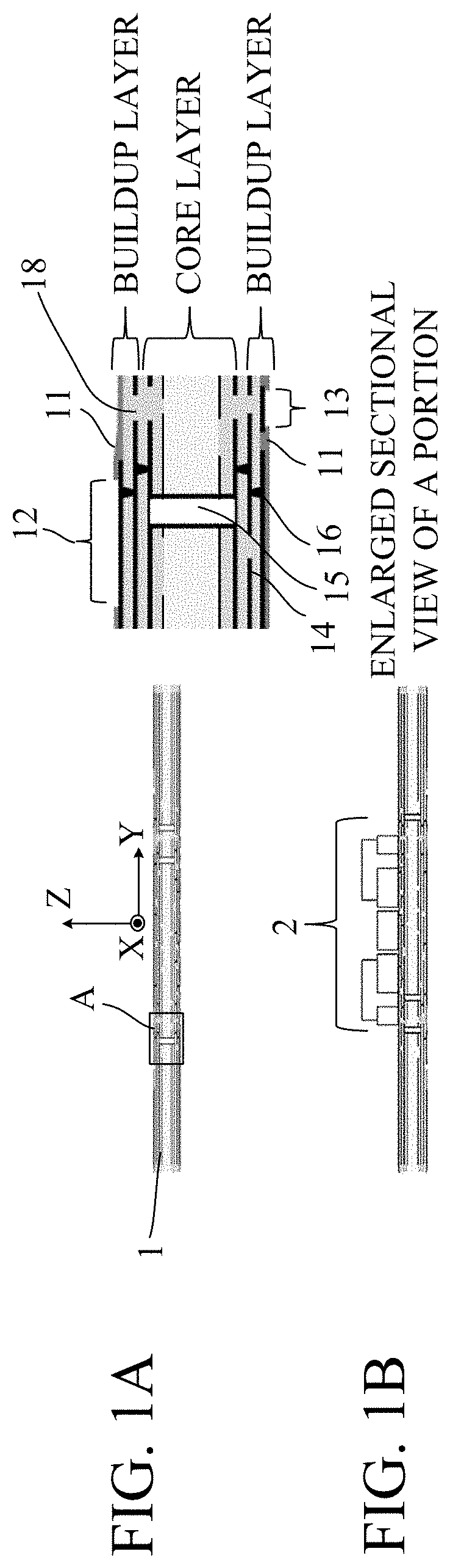
[0020]Referring now to FIGS. 1A to 1B, a description will be given of an image sensor package according to a first embodiment of the present invention. FIGS. 1A and 1B are structural diagrams (sectional views) of a printed circuit board in the image sensor package, and illustrate a process sequence of manufacturing the image sensor package.
[0021]FIG. 1A illustrates a stage in which the printed circuit board 1 is prepared, and is a sectional view of a printed circuit board 1 in a coordinate system XYZ illustrated in the figure. The printed circuit board 1 may be a plate-shaped substrate including a circuit conductor, which is suitable because it can easily use for a circuit conductor, for example, a rigid substrate such as a silicon substrate or a ceramic substrate, or a copper foil whose resin substrate has a low electrical resistance. FIG. 1A illustrates an example in which the resin substrate is used as the printed circuit board 1.
[0022]On the right side of FIG. 1A, a detailed lay...
second embodiment
[0038]Referring now to FIGS. 7A to 7E, a description will be given of an image sensor package according to a second embodiment of the present invention. FIGS. 7A to 7E explain the image sensor package according to this embodiment. FIGS. 7A to 7E correspond to FIGS. 5A to 5E described in the first embodiment, and illustrate the finished image sensor package (having no image sensor) according to this embodiment. Since the method of manufacturing the image sensor package in this embodiment is the same as that in the first embodiment, a description thereof will be omitted.
[0039]The image sensor package according to this embodiment includes a printed circuit board 1 having a plurality of conductor layers 14, and a resin molded portion 4 provided so as to surround the outer circumference of the printed circuit board 1. A conductor layer 141 among the plurality of conductor layers 14 which is closest to the resin molded portion 4 has an underframe conductor layer 1412 in the entire circumf...
third embodiment
[0043]Referring now to FIGS. 8A to 8E, a description will be given of an image sensor package according to a third embodiment of the present invention. FIGS. 8A to 8E explain the image sensor package in this embodiment. FIGS. 8A to 8E correspond to FIGS. 5A to 5E described in the first embodiment, and illustrate the finished image sensor package (having no image sensor) according to this embodiment. Since the method of manufacturing the image sensor package in this embodiment is the same as that in the first embodiment, a description thereof will be omitted.
[0044]The image sensor package according to this embodiment includes a printed circuit board 1 having a plurality of conductor layers 14, and a resin molded portion 4 provided so as to surround the outer circumference of the printed circuit board 1. A conductor layer 141 among the plurality of conductor layers 14 which is closest to the resin molded portion 4 has an underframe conductor layer 1412 in the entire circumference or p...
PUM
 Abstract
Description
Claims
Application Information
 - Generate Ideas
- Intellectual Property
- Life Sciences
- Materials
- Tech Scout
- Unparalleled Data Quality
- Higher Quality Content
- 60% Fewer Hallucinations
Browse by: Latest US Patents, China's latest patents, Technical Efficacy Thesaurus, Application Domain, Technology Topic, Popular Technical Reports.
© 2025 PatSnap. All rights reserved.Legal|Privacy policy|Modern Slavery Act Transparency Statement|Sitemap|About US| Contact US: help@patsnap.com