Electrostatic device for holding an electronic component wafer

Inactive Publication Date: 2006-11-07
SEMCO ENG
View PDF11 Cites 6 Cited by
  • Summary
  • Abstract
  • Description
  • Claims
  • Application Information

AI Technical Summary

Benefits of technology

[0004]The object of the present invention is to provide a device for holding a wafer for supporting particularly electronic components or the like, which permits their manipulation without damage or deformation, and without risk of altering t

Problems solved by technology

The problem arises for holding such slices because of their slight thickness.
More particularly, the thin character of these wafers, of the order of several tens to several hundreds of microns, renders their holding delicate with the risk of deforming them, even altering the components that they support.
However, the development of t

Method used


Image

  • Electrostatic device for holding an electronic component wafer
  • Electrostatic device for holding an electronic component wafer

Examples


Embodiment Construction

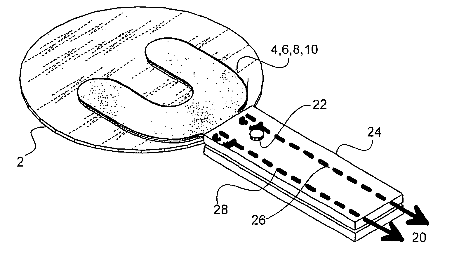
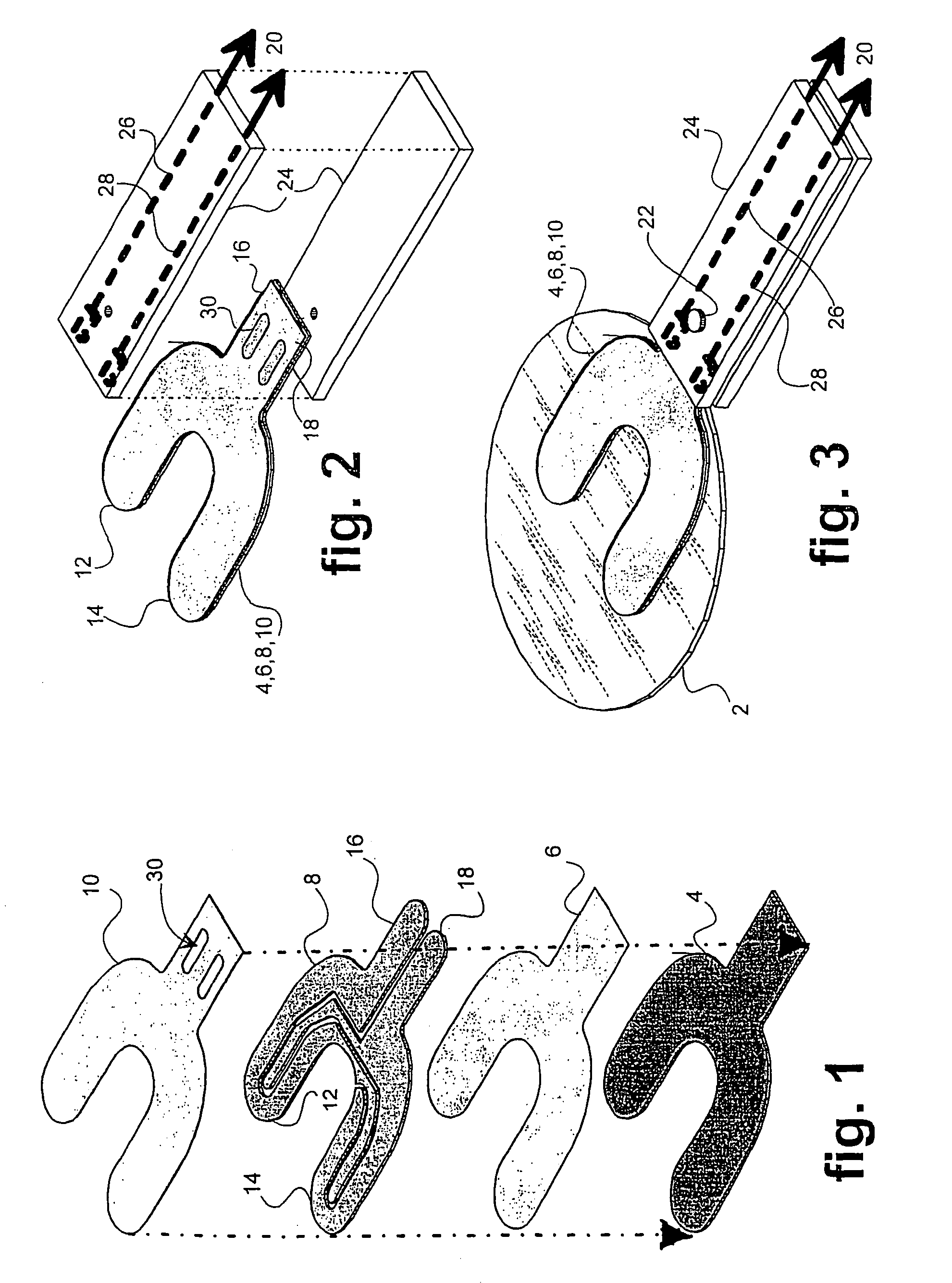
[0019]In the drawings, a device according to the invention for holding a wafer 2, is a layered device comprising successively:[0020]a) a rigid flat support 4, of stainless steel particularly, or of a ceramic insulating material or the like,[0021]b) a first layer of insulating material 6, such as Kapton or any other dielectric material,[0022]c) an electrode 8, of copper or the like,[0023]d) a second layer of insulating material 10, such as Kapton.

[0024]The first layer of Kapton is cemented to the support 4; the electrode is held between the two layers of Kapton 6–10 and the layer 10 of insulating material is, during holding, in contact with the wafer to be manipulated.

[0025]The particular U shaped configuration of the support 4 and of the electrode 8 which it carries, will be noted. Each leg of the U corresponds to a respective branch 12 and 14 of the electrode, prolonged by connection members 16 and 18 of the electrode to a remote source 20 for the support of electricity.

[0026]The s...


PUM


Abstract

A device for holding a wafer, an electronic component comprises a system for transporting without deformation a wafer of electronic components. The device also enables the transport by one or the other of the passive or active faces. The device comprises a planar and thin rigid support having a controllable temperature and at least an electrode consisting of (N+1) elements, confined between two sheets of insulating material. The support provides a protrusion-free surface for gripping the wafer, and electrostatic elements for positive retention of the wafer induces a gripping power of the latter distributed over the entire support. The U-shaped support is borne by the electrical bond of the electrode with a remote (adjustable, AC or DC, mono-multipolar) power source. The gripping surface of the device is planar and protrusion-free whatever the geometry of the support used.

Description

FIELD OF THE INVENTION[0001]The invention is in the field of the technique of manipulating sheet material, more particularly wafers of micrometric electronic components, such as silicon. The invention has for its object a device for holding such material, a so-called wafer.BACKGROUND OF THE INVENTION[0002]It will be recalled, in the field of electronic components, that sheet-like elements called wafers are used, such as of silicon. The problem arises for holding such slices because of their slight thickness. More particularly, the thin character of these wafers, of the order of several tens to several hundreds of microns, renders their holding delicate with the risk of deforming them, even altering the components that they support. At present, these wafers are manipulated by means of their passive surface, to avoid alteration of their other active surface, which supports electronic components.[0003]There is known a technique of holding wafers by suction. For example, the wafer is pr...

Claims


Application Information

Patent Timeline
IPC IPC(8): H01G7/02B25J15/06B65G49/07H01L21/00H01L21/677H01L21/683H01L21/687H02N13/00
CPCH01L21/6831H01L21/68707H02N13/00H01L21/68
Inventor FERRERES, DAVID
Owner SEMCO ENG
Why Eureka
Try Eureka