Complementary zener triggered bipolar ESD protection

a technology of bipolar esd protection and complementary zener, which is applied in the direction of emergency protective circuit arrangements, emergency protective arrangements for limiting excess voltage/current, and emergency protective arrangements for preventing excess voltage/current, etc., which can solve problems such as a number of limitations, easy damage, and high risk of modern integrated circuits

Active Publication Date: 2008-08-28
NXP USA INC
View PDF8 Cites 78 Cited by
  • Summary
  • Abstract
  • Description
  • Claims
  • Application Information

AI Technical Summary

Problems solved by technology

Modern integrated circuits (ICs) are at risk of damage due to electrostatic discharge (ESD) events.
Because the gate dielectric on most MOSFETS is relatively thin, it can be easily damaged if excess voltage appears on the gate terminal.
While such prior art

Method used


Image

  • Complementary zener triggered bipolar ESD protection
  • Complementary zener triggered bipolar ESD protection
  • Complementary zener triggered bipolar ESD protection

Examples


first embodiment

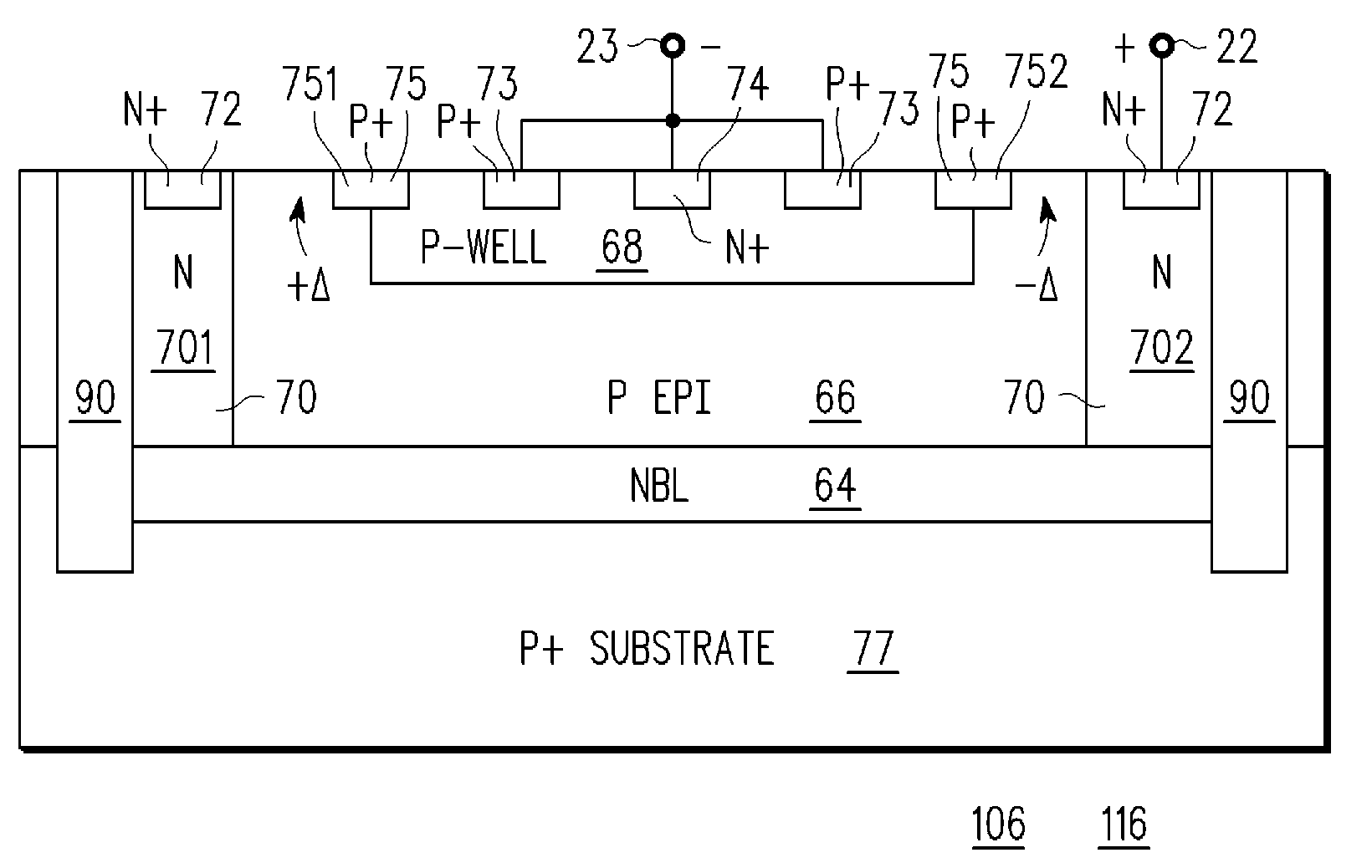
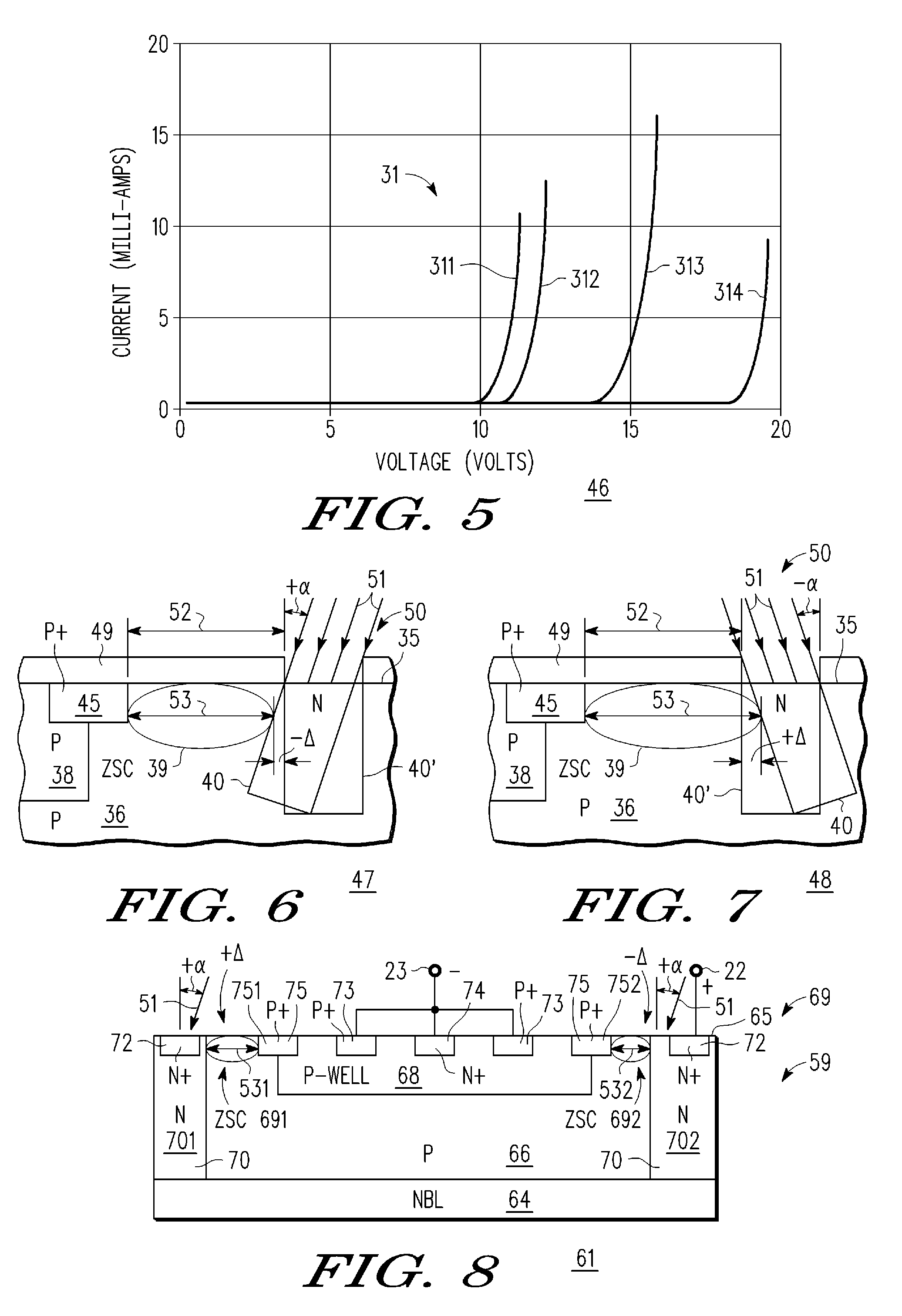
[0034]According to the invention, there is provided an electrostatic discharge (ESD) protection clamp having first and second protective terminals adapted to limit a voltage appearing across protected terminals of an integrated circuit (IC) to which the protective terminals are coupled, comprising, a bipolar transistor having an emitter of a first conductivity type coupled to the first protective terminal, a collector of the first conductivity type coupled to the second protective terminal and a base of a second, opposite conductivity type located between the emitter and collector, an integrated Zener diode having a first Zener terminal of the second conductivity type ohmically coupled to the base and a second Zener terminal of the first conductivity type ohmically coupled to the collector, wherein, the first Zener terminal has a substantially annular ring shape at a periphery of the base, and the second Zener terminal has a substantially annular ring shape spaced apart from the fir...

second embodiment

[0035] there is provided a process for forming an ESD clamp adapted for use in protecting terminals of a semiconductor integrated circuit (IC) from excess voltage, comprising, providing a supporting substrate having a first surface, forming a semiconductor buried layer of a first conductivity type in or on the first surface, forming a semiconductor layer of a second, opposite, conductivity type overlying the buried layer and having an outer surface, angle implanting an annular shaped sinker region of the first conductivity type extending to the buried layer, the annular shaped sinker region being adapted to form a first terminal of an integrated Zener diode, providing a dielectric isolation region laterally outside the annular sinker region, forming a well region of the second conductivity type in the semiconductor layer, extending to the first surface, lying laterally within and spaced apart from the annular shaped sinker region, forming an emitter region of the first conductivity ...

third embodiment

[0036] there is provided an ESD clamp, comprising, a bipolar transistor having an emitter region, a collector region and a base region, an integrated Zener comprising a first terminal and second terminal, the first terminal integral with a part of the base region and the second terminal integral with a part of the collector region, wherein the second terminal has an annular shape laterally surrounding and spaced apart from the base region, and wherein the first terminal has an annular shape lying laterally within and laterally separated from the second terminal and laterally surrounding and ohmically coupled to the base region. According to a further embodiment, an annular shaped space of predetermined width separates the first and second terminals of the Zener, and wherein the predetermined width has a first value on one side of the bipolar transistor and a second value on an opposite side of the bipolar transistor. According to a still further embodiment, the second terminal is fo...


PUM


Abstract

An electrostatic discharge (ESD) protection clamp (61) for I/O terminals (22, 23) of integrated circuits (ICs) (24) comprises an NPN bipolar transistor (25) coupled to an integrated Zener diode (30). Variations in the break-down current-voltage characteristics (311, 312, 313, 314) of multiple prior art ESD clamps (31) in different parts of the same IC chip is avoided by forming the anode (301) of the Zener (30) in the shape of a base-coupled P+ annular ring (75) surrounded by a spaced-apart N+ annular collector ring (70) for the cathode (302) of the Zener (30). Even though an angled implant (51, 86, 98) used to form the N+ annular collector ring (70) causes location dependent variations in the width (53) of the Zener space charge (ZSC) region (69), the improved annular shaped clamp (61) always has a portion that initiates break-down at the design voltage so that variations in the width (53) of the ZSC region (69) do not cause significant variations in the clamp's current-voltage characteristics (611, 612, 613, 614).

Description

FIELD OF THE INVENTION[0001]The present invention generally relates to semiconductor devices and methods for fabricating semiconductor devices, and more particularly relates to semiconductor devices used for electrostatic discharge (ESD) protection in integrated circuits.BACKGROUND OF THE INVENTION[0002]Modern integrated circuits (ICs) are at risk of damage due to electrostatic discharge (ESD) events. This is especially true of ICs that use field effect transistors (FETs), especially metal oxide semiconductor field effect transistors (MOSFETs), or simply MOS transistors or devices. Although the term “MOS” properly refers to a device having a metal gate electrode and an oxide gate insulator, that term is also used to refer to any semiconductor device that includes a conductive gate electrode (whether metal or not) that is positioned over a gate insulator (whether oxide or other dielectric material) which, in turn, is positioned over a semiconductor surface. Accordingly, the terms met...

Claims


Application Information

Patent Timeline
IPC IPC(8): H01L23/62H01L21/8222
CPCH01L27/0259H01L2924/0002H01L2924/00
Inventor XU, HONGZHONGGILL, CHAI EANWHITFIELD, JAMES D.YANG, JINMAN
Owner NXP USA INC
Why Eureka
Try Eureka