Anti-ESD photomask blank

a photomask and anti-esd technology, applied in the field of photomasks, can solve the problems of electrostatic discharge on the photomask, easy damage to the reticle and the photomask, and melting a circuit line and destroying the circuit pattern, so as to reduce the delay in the photomask cycle time due to electrostatic discharge and enhance the quality of the photomask

Active Publication Date: 2006-07-13
TAIWAN SEMICON MFG CO LTD
View PDF5 Cites 77 Cited by
  • Summary
  • Abstract
  • Description
  • Claims
  • Application Information

AI Technical Summary

Benefits of technology

[0010] The present invention is generally directed to a novel anti-ESD photomask blank which can be used for the fabrication of an anti-ESD photomask. The anti-ESD photomask blank includes a transparent mask substrate, a conductive layer provided on the mask substrate, an patterning layer such as chromium provided on the conductive layer and a photoresist layer provided on the patterning layer. An anti-ESD mask can be fabricated from the anti-ESD mask blank by exposure, baking and development, respectively, of the photoresist layer; etching of the patterning layer according to the pattern defined by the photoresist layer to define a patterned layer having the desired circuit pattern; and stripping of the photoresist layer from the patterned layer. The conductive layer establishes electrical continuity between all areas or regions of the patterned layer, thus preventing the formation of voltage differences on the patterned layer which could cause electrostatic discharges that could damage the photomask. Consequently, photomask quality is enhanced and photomask cycle time delay due to electrostatic discharges is reduced.

Problems solved by technology

Reticles and photomasks may be easily damaged such as by dropping, by the formation of scratches on the reticle or photomask surface, electrostatic discharge (ESD), and particles.
ESD can cause discharge of a small current through the chromium lines on the surface of the reticle or photomask, melting a circuit line and destroying the circuit pattern.
Voltage differences are frequently established between adjacent portions of a patterned chromium layer on a photomask, resulting in electrostatic discharges on the photomask.
Consequently, the circuit pattern image transferred through the mask can be distorted, compromising pattern reliability and causing severe yield loss.

Method used


Image

  • Anti-ESD photomask blank
  • Anti-ESD photomask blank
  • Anti-ESD photomask blank

Examples


Embodiment Construction

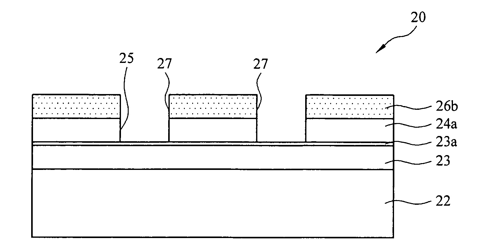
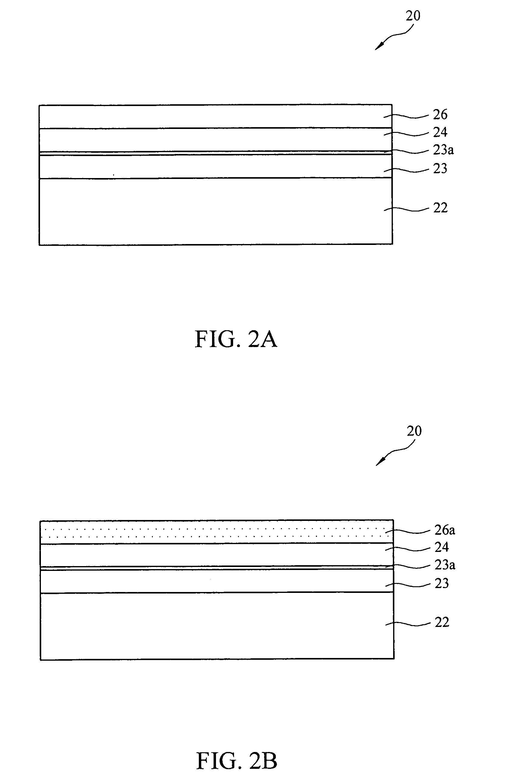
[0016] The present invention contemplates a novel anti-ESD photomask blank which is used as the starting material for the fabrication of an anti-ESD photomask. The anti-ESD photomask blank includes a transparent mask substrate such as quartz or fused silica. An electrically-conductive layer is provided on the mask substrate. An opaque patterning layer, which may be chromium, for example, is provided on the conductive layer, and a photoresist layer is provided on the patterning layer. An anti-ESD photomask is fabricated from the anti-ESD mask blank typically using conventional fabrication techniques, with the patterning layer etched into a patterned layer having the desired circuit pattern. During storage, transport or use of the anti-ESD photomask, the conductive layer establishes electrical communication between all areas or regions of the patterned layer, thus preventing the formation of voltage differences on the patterned layer which could cause electrostatic discharges that cou...


PUM

PropertyMeasurementUnit
thicknessaaaaaaaaaa
diameteraaaaaaaaaa
wavelengthaaaaaaaaaa

Abstract

An anti-electrostatic discharge photomask blank for fabrication of an anti-electrostatic discharge photomask is disclosed. The anti-electrostatic discharge photomask blank includes a mask substrate, a conductive layer provided on the mask substrate and an opaque patterning layer provided on the conductive layer. The conductive layer prevents charges of opposite polarity from accumulating on a photomask fabricated from the photomask blank, thus preventing electrostatic discharges on the photomask.

Description

FIELD OF THE INVENTION [0001] The present invention relates to photomasks used to transfer circuit patterns onto semiconductor wafers in the fabrication of integrated circuits. More particularly, the present invention relates to an anti-electrostatic discharge (ESD) photomask blank for fabrication of a photomask, which anti-ESD photomask blank includes a conductive layer interposed between a patterning layer such as chromium and a mask substrate to eliminate electrostatic discharges on the photomask. BACKGROUND OF THE INVENTION [0002] The fabrication of various solid state devices requires the use of planar substrates, or semiconductor wafers, on which integrated circuits are fabricated. The final number, or yield, of functional integrated circuits on a wafer at the end of the IC fabrication process is of utmost importance to semiconductor manufacturers, and increasing the yield of circuits on the wafer is the main goal of semiconductor fabrication. After packaging, the circuits on ...

Claims


Application Information

Patent Timeline
Patent Type & Authority Applications(United States)
IPC IPC(8): B32B9/00B32B17/10B32B17/06G03F1/00
CPCG03F1/40G03F1/50G03F1/78Y10T428/31616
Inventor CHIANG, ERICWANG, HUNG-CHUNHSIEH, MIN-CHIHHO, MING-TAO
Owner TAIWAN SEMICON MFG CO LTD
Why Eureka
Try Eureka