Low triggering voltage SOI silicon-control-rectifier (SCR) structure

Inactive Publication Date: 2001-06-05
UNITED MICROELECTRONICS CORP
View PDF2 Cites 78 Cited by
  • Summary
  • Abstract
  • Description
  • Claims
  • Application Information

AI Technical Summary

Benefits of technology

An object of the present invention is to substantially obviate one or more

Problems solved by technology

However, with power supply reduction, transistor performance is severely impacted by both junction capacitance and the MOSFET body effect at lower voltages.
As technologies scale below 0.25 .mu.m channel lengths, to 0.15 and 0.1 .mu.m, short-channel effects (SCE) control, gate resistance, channel profiling and other barriers become an issue for advanced CMOS technologies.
While significant success has been achieved with successive scaling of bulk CMOS technology, the ma

Method used


Image

  • Low triggering voltage SOI silicon-control-rectifier (SCR) structure
  • Low triggering voltage SOI silicon-control-rectifier (SCR) structure
  • Low triggering voltage SOI silicon-control-rectifier (SCR) structure

Examples


Embodiment Construction

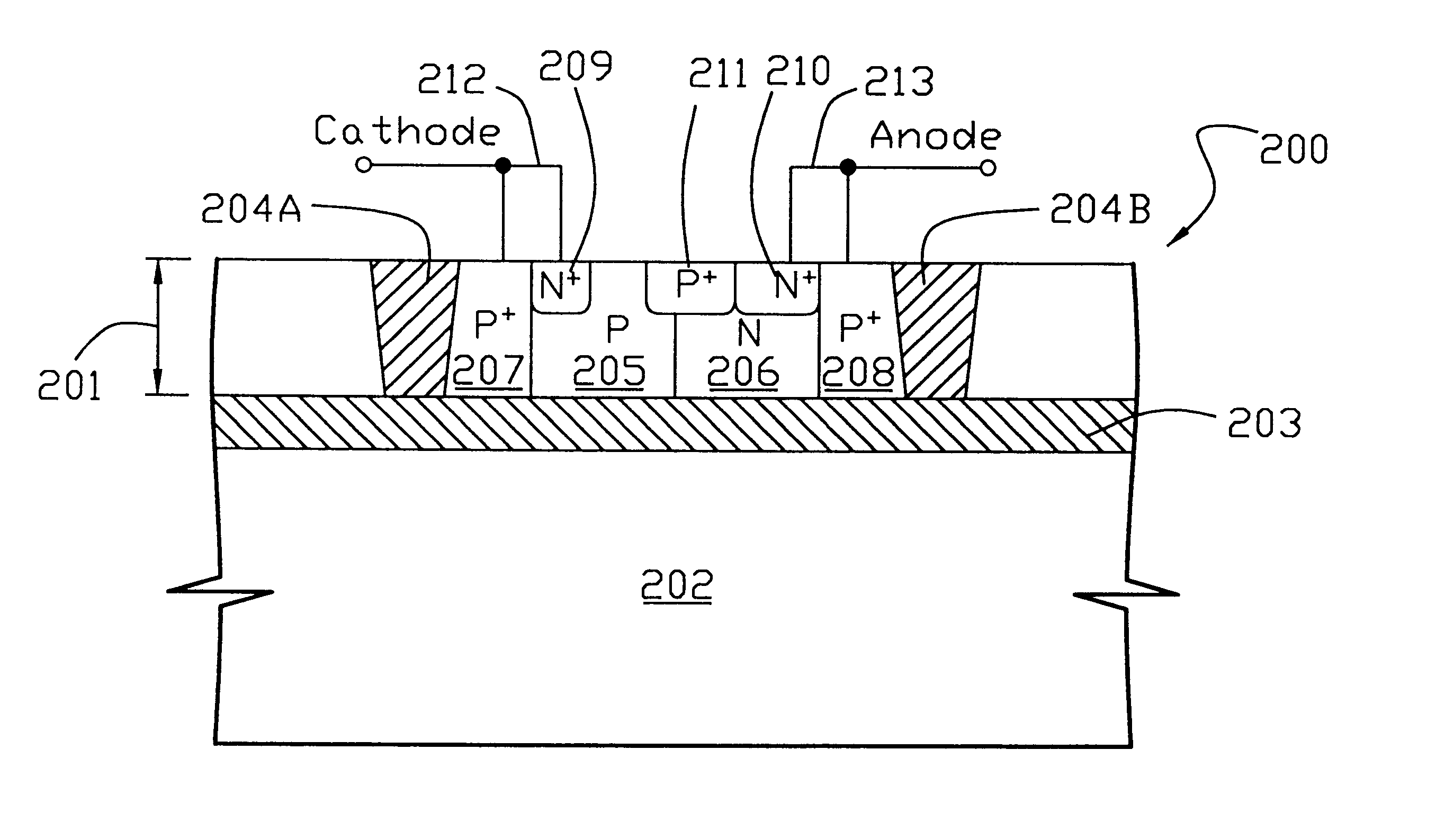
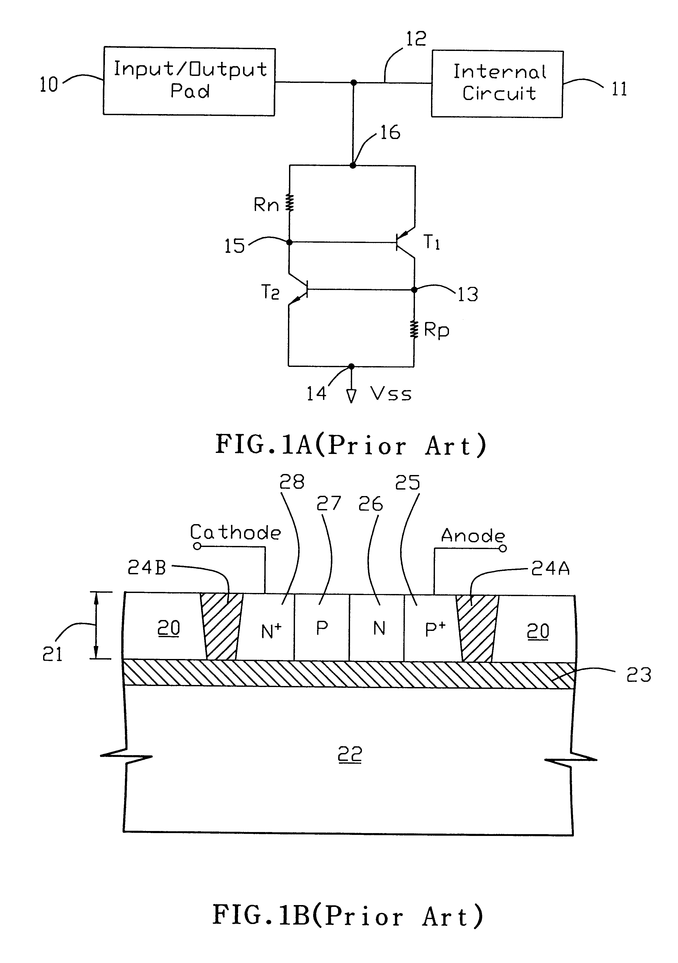
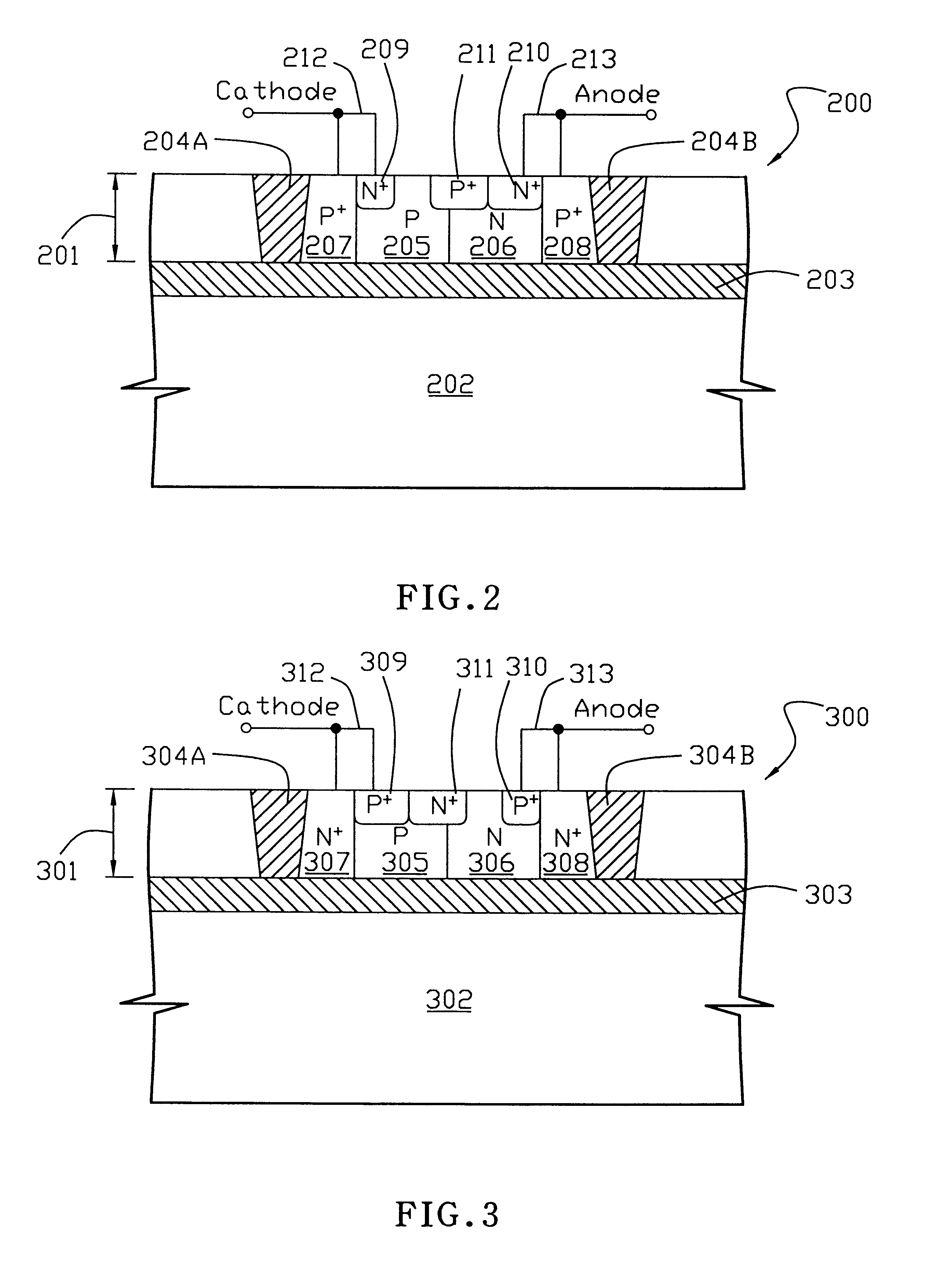
Referring to FIG. 2, an arrangement for providing a low voltage trigger source for a protective PD-SOI (Partially-Depleted Silicon-on-Insulator) SCR (Silicon-Control-Rectifier) in accordance with an embodiment of the present invention is shown, wherein an improved low voltage trigger source is produced for the PD-SOI SCR by using a zener diode N.sup.+ -P.sup.+ junction under a reverse bias. A semiconductor substrate 200 is firstly provided having a thin film layer 201 with a thickness of more than about 1000 angstroms separated from a bulk silicon substrate 202 by a buried oxide insulator 203 inside the semiconductor substrate 200. A first shallow trench isolation (STI) region 204A, preferably composed of silicon dioxide, is formed within the thin film layer 201 and at a certain distance away from the first STI region 204A where a second STI region 204B is formed. Both the first and second STI regions have a vertical depth equal to the thickness of the thin film layer 201, that is, ...


PUM


Abstract

A low triggering voltage PD-SOI (Partially-Depleted Silicon-on-Insulator) electrostatic discharge (ESD) protection structure is disclosed. In one embodiment, the protection structure includes: A semiconductor substrate; a thin film layer separated from a bulk silicon substrate by an insulator inside the semiconductor substrate; a first isolation region formed in the thin film layer; a second isolation region formed in the thin film layer; a first region having a first conductivity type formed in between the first and second isolation region; a second region formed in between the first region and the second isolation region, the second region being of a second conductivity type; a third region formed in between the first isolation region and the first region, the third region being of the first conductivity type; a fourth region formed in between the second isolation region and the second region, the fourth region being of the first conductivity type; a fifth region having an exposed upper surface formed in the first region, the fifth region being of the second conductivity type; a sixth region having an exposed surface formed in the second region, the sixth region being of the second conductivity type; and a seventh region having an exposed upper surface formed in the second region and overlapping the first region, moreover, the seventh region being between the fifth and sixth region and the seventh region being of the first conductivity type. Another embodiment of the present invention is very similar to the previous one, which is also extracted in the present specification.

Description

BACKGROUND OF THE INVENTION1. Field of the InventionThe present invention relates to an apparatus for electrostatic discharge (ESD) protection in silicon-on-insulator (SOI) technologies and, more particularly, to a low triggering voltage partially-depleted (PD) SOI silicon-control-rectifier (SCR) structure.2. Description of the Prior ArtMetal oxide semiconductor field effect transistor (MOSFET) scaling on bulk silicon has been the primary focus of the semiconductor and microelectronic industry for achieving complementary metal oxide semiconductor (CMOS) chip performance and density objectives. The shrinking of MOSFET dimensions for high density, low power and enhanced performance requires reduced power-supply voltages. Because power consumption (P) is a function of capacitance (C), power supply voltage (V), and transition frequency (f), in accordance with the expression P=CV.sup.2 f, the focus has been on reducing both C and V as the transition frequency f increases. As a result, di...

Claims


Application Information

Patent Timeline
IPC IPC(8): H01L27/02H01L29/66H01L29/87
CPCH01L27/0262H01L29/87
Inventor CHEN, SHIAO-SHIENTANG, TIEN-HAOCHOU, JIH-WENWANG, MU-CHUN
Owner UNITED MICROELECTRONICS CORP
Why Eureka
Try Eureka