Conformal mesh for thermal imaging

a technology of thermal imaging and mesh, applied in the direction of positive temperature coefficient thermistors, instruments, heat measurement, etc., can solve the problems of inability to stretch or conform to accommodate three-dimensional objects, failure to fulfill the role of “skins", and limited conformability, so as to reduce the total number of thermal resistors, and improve the effect of thermal sensing performan

Active Publication Date: 2010-08-03
THE BOARD OF TRUSTEES OF THE UNIV OF ILLINOIS
View PDF11 Cites 6 Cited by
  • Summary
  • Abstract
  • Description
  • Claims
  • Application Information

AI Technical Summary

Benefits of technology

[0006]The present invention relates to a thermal sensor that comprises a micromachined thermal imaging mesh for conformal sensing. The devices and methods of the present invention rely on patterned rows and columns of thermal resistors to significantly decrease the total number of thermal resistors required for thermal imaging. The thermal sensor is flexible and extensible and, thus, capable of stretching without damage or significant degradation in sensor performance. The thermal sensors of the present invention are capable of mechanical deformations to cover contoured surfaces conformally, including curved surfaces having a large radius of curvature. Thermal sensors of the present invention may be free standing and capable of efficient integration with a range devices and device components, including integrated sensors, actuators, electronic circuits, power supplies and displays. Furthermore, the thermal sensors of the present invention are capable of integration with various fabrics, woven networks and / or mesh network of elements.
[0007]An object of the present invention is to provide versatile methods of making flexible thermal sensors having a wide range of physical dimensions, including sensors and sensor combinations capable of thermally imaging regions having a wide range of surface areas, including large surface areas, such as surface areas between about 10 mm2 and about 1 m2. The present invention further provides methods of thermal sensing from thermal sensors having a reduced number of thermal resistors while still maintaining acceptable thermal resolution.
[0008]In an embodiment, the thermal sensor comprises one layer of thermal resistors of number m, and a second layer of thermal resistors of number n, to generate a thermal image comprising m*n data points. For large m and / or n, this provides a significant decrease in the number thermal sensors compared to instruments that use one thermal resistor for each data point entry of the m×n matrix (e.g., m+n<m*n). The sensing and processing schemes of the present invention are versatile and permit thermal imaging over small or large regions, including solid surfaces having curved, planar, or curved and planar contour profiles. The sensor is particularly useful in the presence of a localized heat source over a broad piece of imaging mesh. At the same time, this approach dramatically reduces the number of sensors, and hence the wiring required to image a given area.
[0010]The thermal resistors can comprise metals whose resistance changes with temperature. Gold is a particularly useful metal as it is compatible with anisotropic conductive film for connecting the thermal resistor to outside electrical connections. Gold is also stable and relatively resistant to corrosion. In an exemplified embodiment, the polymer layers are made from polyimide. Polyimide polymer layers are sufficiently flexible to facilitate conformal contact with a three-dimensional surface, such as a portion of a sphere surface. To further facilitate sensor flexibility, thermal resistors that are wires can comprise curved portions to minimize stress in the thermal resistors as the sensor deforms. In an aspect, the thermal resistors are curved, periodically curved or serpentine. In an aspect, the devices of the present invention comprise polymer layers having a thickness, such that the total thickness of a thermal sensor of the present invention is less than about 20 μm, and each of the top and bottom polymer layers have a thickness ranging from 3 μm to 10 μm, 5 μm to 7 μm, or about 6 μm. The insulative layer separating the top and bottom layers preferably has a smaller thickness than the top and bottom layers, including ranging from between 0.5 μm and 3 μm, or about 1 μm.
[0013]In an embodiment, the thermal sensor is a free-standing conformable mesh comprising layers of flexible polyimide fabric, with a first pattern of thermal resistors between the first and insulative polyimide layers and a second pattern of thermal resistors between the insulative and second polyimide layers, wherein the first and second patterns are in a row and column (or vice versa) configuration. Thermal resistors having serpentine structure further improve the conformability of the fabric to three-dimensional objects. In an exemplified embodiment, the thermal resistors are gold wires about 50 μm wide and 5000 Å in depth, the outside polyimide layers are about 6 μm thick, and the insulative layer separating the thermal resistor layers is about 1 μm, so that the free-standing mesh thermal sensor is about 13 μm thick. The flexible free standing structures of the present invention also provide thermal sensing and regulation systems for selectively conducting and distributing thermal energy. The “insulative layer” refers to a layer that is an electrical insulator (e.g., a substance that is highly resistant to electric current), such as a dielectric material. In the thermal sensing embodiment, the layers are preferably thermally conductive to maximize thermal resolution and sensitivity.
[0017]The invention, in an embodiment, removes the sacrificial layer to release the first patterned thermal resistor structural layer, thereby obtaining a free-standing thermal sensing mesh. A free-standing thermal sensing mesh having layers made from flexible polymers is capable of conforming to a contoured surface. Any of the thermal sensors and methods of making such thermal sensors can comprise one or more additional layers of thermal resistors to further enhance thermal sensing and imaging.

Problems solved by technology

Even though these devices are able to achieve some degree of conformability, the conformability is restricted to simple curvatures like a cylinder.
They cannot stretch or conform to accommodate three-dimensional objects like a sphere, and thus fail to fulfill their roles as “skins”.
This does not only apply to thermal sensing, but also more generally to when a localized input is acquired over a relatively sensing area, and usually involves large number of sensor arrays, cumbersome wiring and complicated test setup.
Those devices, however, are rather limited in their ability to sense spatial thermal distribution over a surface, including a planar, non-planar or bent surface.
That sensor, however, requires a large number of thermal sensors and associated wiring in order to obtain an accurate thermal image.
Previously disclosed temperature sensors generally suffer the drawback of requiring an excessive number of thermal sensing elements to adequately resolve a thermal image.
Further, many conventional temperature sensors lack the mechanical conformability required to provide accurate measurement of temperature distributions of non-planar (e.g., curved) surfaces.

Method used


Image

  • Conformal mesh for thermal imaging
  • Conformal mesh for thermal imaging
  • Conformal mesh for thermal imaging

Examples


example 1

Array Methodology for Thermal Sensing

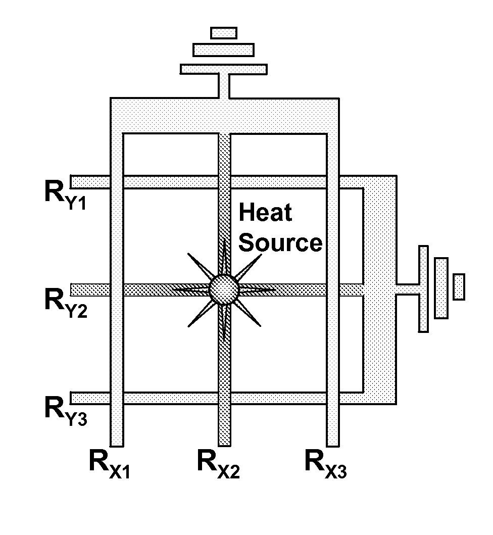
[0054]The thermal sensing mesh consists of an m-by-n matrix of gold thermal resistor network. But instead of having m×n number of individually addressable sensors, only m+n number of sensors are used to address the individual entries of the m-by-n matrix. The significance of this sensor configuration is obvious at large values of m and / or n.

[0055]The sensing of a localized heat source is accomplished by the joint entry of two layers of insulated thermal sensors. The bottom layer consists of m rows of gold thermal resistor named Ry1 to Rym; the top layer consists of n columns of thermal resistor named Rx1 to Rxn (see FIG. 1A for n=m=3). Consider an ideal localized heat source over the point (i, j) on the matrix. As a consequence of the elevated temperature, the corresponding Ryi and Rxj of the thermal resistors increases. The percentage change of resistance is calculated and recorded. The entry Z(i, j) is determined by the product of the percentag...

example 2

Fabrication of Conformable Array

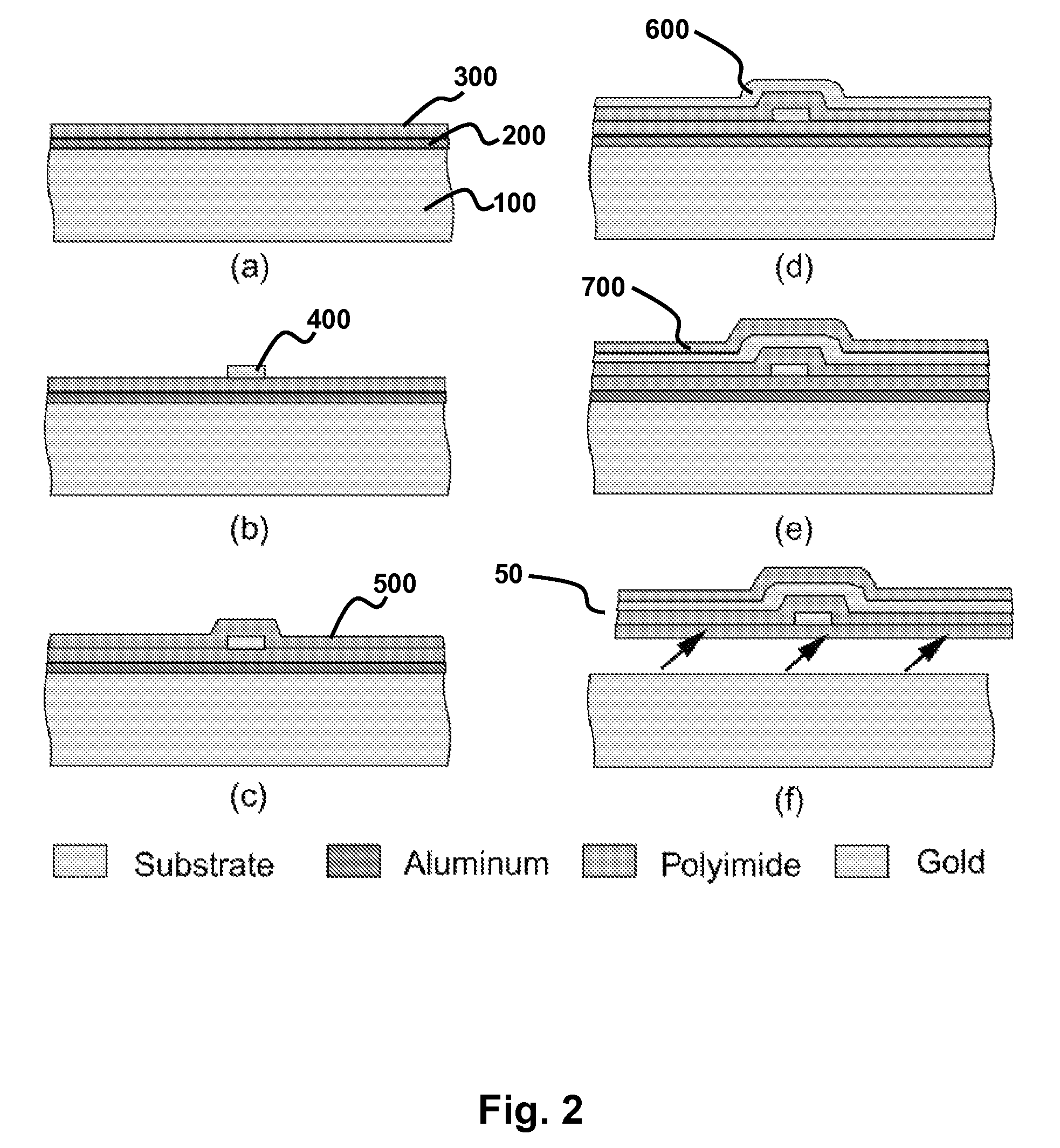
[0059]An example of a fabrication process for making a thermal imaging mesh is summarized in FIG. 2. First, 2000 Å of Al is evaporated onto a 2-inch Si wafer 100 as sacrificial layer 200. On top of the Al layer 200, a first layer of polyimide 300 is spun on, patterned and cured (FIG. 2A). The resultant thickness is about 6 μm. This thick layer of polyimide serves as the base structural layer of the fabric. Then the first layer of 5000 Å gold is evaporated and patterned into 50 μm wide lines 400. These resistor lines form the rows of the thermal resistor network (FIG. 2B). On top of the first gold layer, a second layer of polyimide 500 is spun on, patterned and cured. The resultant thickness is about 1 μm (FIG. 2C). This thin layer of polyimide serves as the insulation layer 500 between the first and second layer of gold thermal resistors. Following the insulation layer, the second layer of 5000 Å gold is evaporated and patterned into 50 μm wide lines ...

example 3

Thermal Imager Testing

[0065]Packaging: A 25×25 matrix thermal imaging mesh is tested. Instead of 625 individual thermal sensors, only 50 thermal sensors are used to address the individual entries of the 25×25 matrix. The number of sensors required and corresponding wiring is greatly reduced.

[0066]The sample is about 5 cm long across the diagonal. To simplify testing, the sample is packaged to a PCB board with wires routed to 25-pin cable connectors (FIG. 7A). A square opening approximately the size of the sample is first milled out from the PCB board. Electrical connections between the mesh and the PCB board are then achieved using methods known in the art such as ACF (anisotropic conductive film). ACF is originally developed for the LCD panel industry and is useful for electrically connecting flexible structures to rigid surfaces. It exhibits excellent conductivity in the vertical direction in contrast to very large resistance in the lateral direction. It is an excellent solution t...


PUM

PropertyMeasurementUnit
widthaaaaaaaaaa
widthaaaaaaaaaa
thicknessaaaaaaaaaa

Abstract

This invention provides thermal sensors and imagers that are flexible and capable of conforming to curved surfaces and corresponding methods of making and methods of thermal sensing. The thermal sensors contain an array of thermal resistors patterned in a row and column configuration, with each thermal resistor electrically isolated from other thermal resistors within the sensor. Thermal information is obtained from a region by measuring the resistance of each thermal resistor and calculating a thermal resistance for each entry of the array.

Description

CROSS-REFERENCE TO RELATED APPLICATIONS[0001]This application claims benefit of U.S. Provisional Patent Application 60 / 863,702 filed on Oct. 31, 2006 and is incorporated by reference in its entirety.BACKGROUND OF THE INVENTION[0002]The present invention is in the field of conformal thermal sensing and imaging. Conformal temperature sensing has applications in a number of fields. Conformal sensing of various physical parameters is ongoing. A number of researchers have used micromachining techniques to develop sensitive skin sensors for robotics. Flexible multimodal polymer sensor arrays have been realized as well as shear sensor arrays with embedded silicon elements. Even though these devices are able to achieve some degree of conformability, the conformability is restricted to simple curvatures like a cylinder. They cannot stretch or conform to accommodate three-dimensional objects like a sphere, and thus fail to fulfill their roles as “skins”. Other researchers have explored embedd...

Claims


Application Information

Patent Timeline
Patent Type & Authority Patents(United States)
IPC IPC(8): H01C7/10
CPCG01K7/22G01K7/226G01K2213/00
Inventor LIU, CHANGCHEN, NANNANENGEL, JONATHANCHEN, JACKFAN, ZHIFANG
Owner THE BOARD OF TRUSTEES OF THE UNIV OF ILLINOIS
Why Eureka
Try Eureka