Eureka AIR delivers breakthrough ideas for toughest innovation challenges, trusted by R&D personnel around the world.

Display device and manufacturing method thereof

Inactive Publication Date: 2021-09-09
WUHAN CHINA STAR OPTOELECTRONICS SEMICON DISPLAY TECHCO LTD
View PDF0 Cites 1 Cited by
  • Summary
  • Abstract
  • Description
  • Claims
  • Application Information

AI Technical Summary

Benefits of technology

The present invention is a display device and a manufacturing method that can align openings in layers with precision. This is achieved by forming a transparent release agent layer on a camera region of a cover plate and integrating a manufactured display function structural layer on top of the cover plate. Additionally, a second through hole is defined all layers of the display function structural layer with the same size and shape as the first through hole in the camera region. This eliminates the need for an aligning step when creating through holes, resulting in improved alignment precision and increased effective area of the displaying region.

Problems solved by technology

How to set a front camera while achieving the full screen is the difficulty of such technology.
The front camera requires the display screen to preserve a transparent region in the display screen to allow light to pass therethrough, and the display screen cannot display images in this region, which lowers the screen ratio.
During Bonding an optical adhesive layer, a polarizer and a backplate each of which has a hole, particle pollution occurs, bonding pictures cannot be precisely aligned, an edge of the hole has cracks due to stress, which makes the process difficult.
Because of the bonding process, a tolerance increased, a misalignment region of edges of the holes increases such that the holes are difficult to be aligned with one another, which decreases an effective area of a displaying region of the display screen.

Method used


Image

  • Display device and manufacturing method thereof
  • Display device and manufacturing method thereof
  • Display device and manufacturing method thereof

Examples


Embodiment Construction

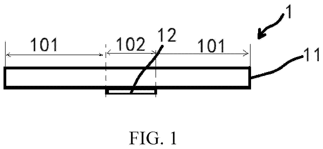
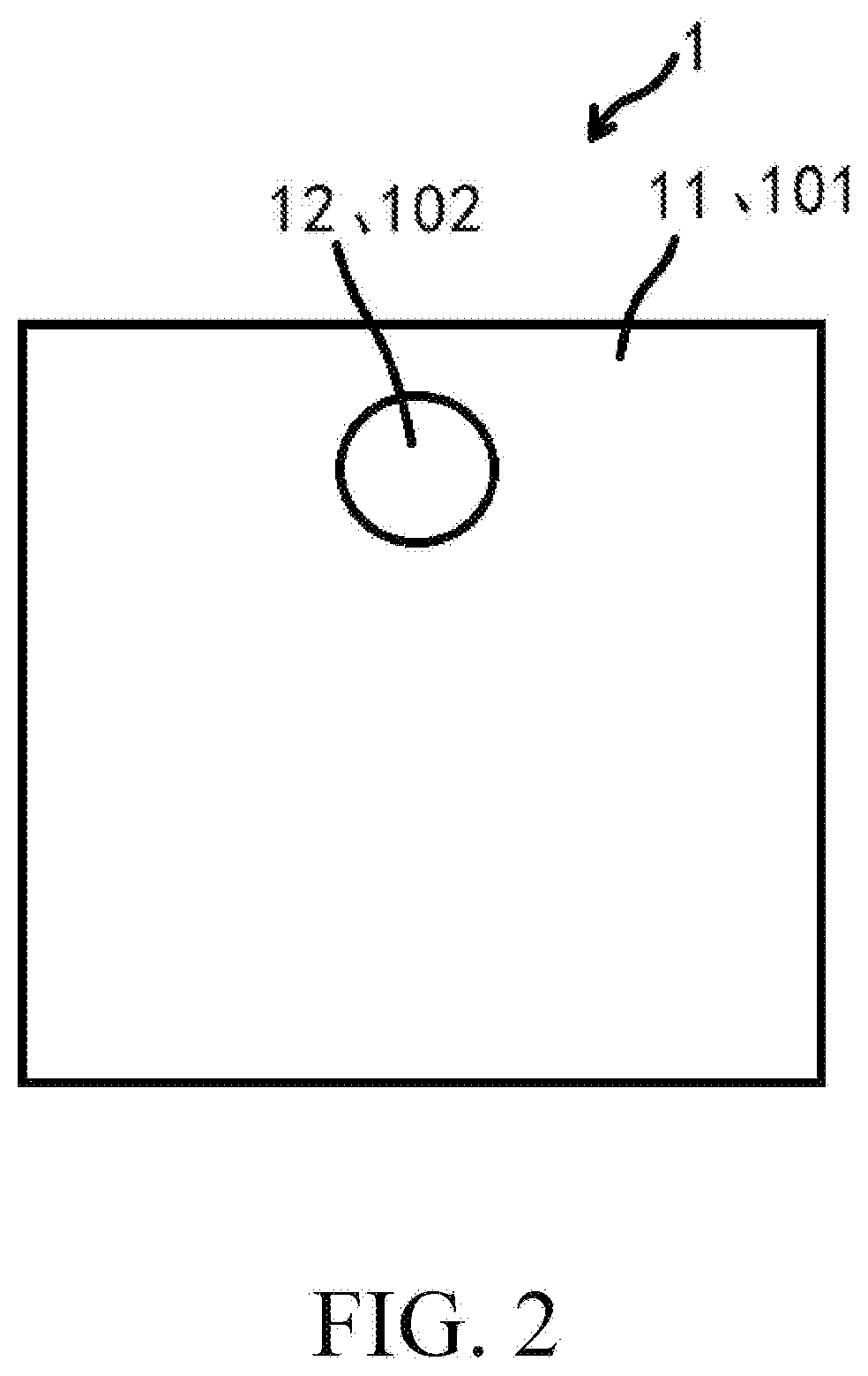
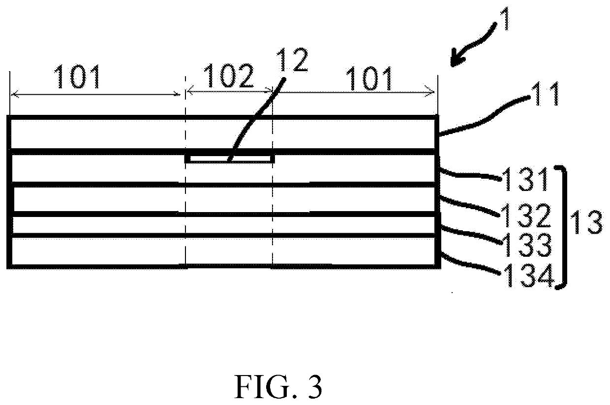
[0031]Embodiments of the present invention will be described in details. Examples of the embodiments are illustrated in the accompanying drawings. The same or similar reference characters refer to the same or similar elements or elements including the same or similar functions. The following embodiments described with reference to the accompanying drawings are exemplary, are only configured to construe the present invention and cannot be understood as limitations to the present invention.

[0032]The embodiments as follows refer to the accompanying drawings for illustrating specific embodiments of the present invention that can be embodied. Directional terminologies mentioned by the present invention, for example “upper”, “lower”, “front”, “rear”, “left”, “right”, “top”, “bottom”, etc., only refer to directions of the accompanying drawings. Therefore, the employed directional terminologies are configured to indicate and make understanding for the present invention but is not for limiti...


PUM


Abstract

The present invention discloses a display device and a manufacturing method thereof, the display device has a camera region and a displaying region surrounding the camera region, and has a cover plate; a transparent release agent layer disposed on the cover plate and is located in the camera region; a display function structural layer disposed on a surface of the cover plate with the transparent release agent layer; a protective adhesive layer disposed on the display function structural layer, and the protective adhesive layer having a first through hole corresponding to a region of the transparent release agent layer; the display function structural layer having a second through hole corresponding to the region of the transparent release agent layer.

Description

CROSS-REFERENCE TO RELATED APPLICATIONS[0001]The application is the National phase under 35 U.S.C. § 371 of International Application No. PCT / CN2019 / 115595, filed Nov. 5, 2019, which claims the benefit of and priority to Chinese Patent Application No. 201910922114.4, filed Sep. 27, 2019. The entire contents of these patent applications are hereby incorporated by reference herein.FIELD OF INVENTION[0002]The present invention relates to a field of display technologies, especially to a display device and a manufacturing method thereof.BACKGROUND OF INVENTION[0003]With development of technologies, and people's increasing requirements for products, a full screen with higher screen ratio becomes the most expected developing trend of smart phones. How to set a front camera while achieving the full screen is the difficulty of such technology. The front camera requires the display screen to preserve a transparent region in the display screen to allow light to pass therethrough, and the displ...

Claims


Application Information

Patent Timeline
IPC IPC(8): G02F1/1333G02F1/1335
CPCG02F1/13338G02F1/133314G02F1/133531G02F1/1333G02F1/133308G02F2202/28G02F1/13312
Inventor ZHAN, DONGLI, WUYANG, HAMNING
Owner WUHAN CHINA STAR OPTOELECTRONICS SEMICON DISPLAY TECHCO LTD
Why Eureka
Eureka Blog
Learn More