
System and method for radical and thermal processing of substrates

Pending Publication Date: 2021-09-09
APPLIED MATERIALS INC
View PDF5 Cites 1 Cited by
  • Summary
  • Abstract
  • Description
  • Claims
  • Application Information

AI Technical Summary

Benefits of technology

The patent describes a method of processing a substrate to create a 3D memory structure. The substrate is exposed to a hydrogen or deuterium plasma in a vacuum chamber and annealed to form a nucleated substrate. This nucleated substrate is then further heated to create a final product. The key technical effect is that this method creates a substrate with high aspect ratio features, such as in a 3D memory structure, with improved uniformity and reduced damage.

Problems solved by technology

Moreover, manufacturers are continuously increasing the height of the stacks which increases the length of the channel.
The speed of the device becomes limited by the mobility of electrons in the channel and the increased lengths that the electrons must travel.
Such processes, however, are not ideal because annealing alone causes high thermal budgets which include running at high temperatures for long residence times. Temperature is often limited because exceeding certain temperatures can cause defects in the device.
If residence time and / or temperature is inadequate, then grain sizes do not grow to an adequate level and can produce devices with poor performance.

Method used


Image

  • System and method for radical and thermal processing of substrates
  • System and method for radical and thermal processing of substrates
  • System and method for radical and thermal processing of substrates

Examples


Embodiment Construction

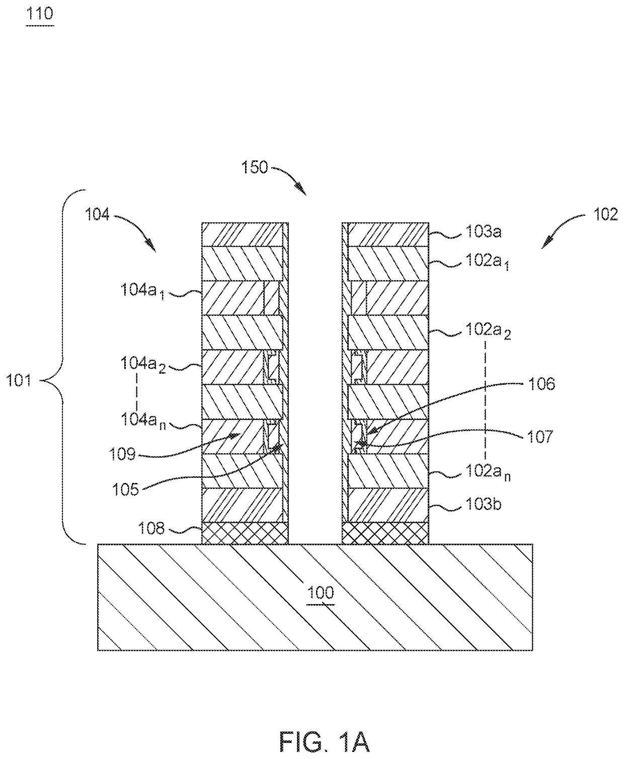
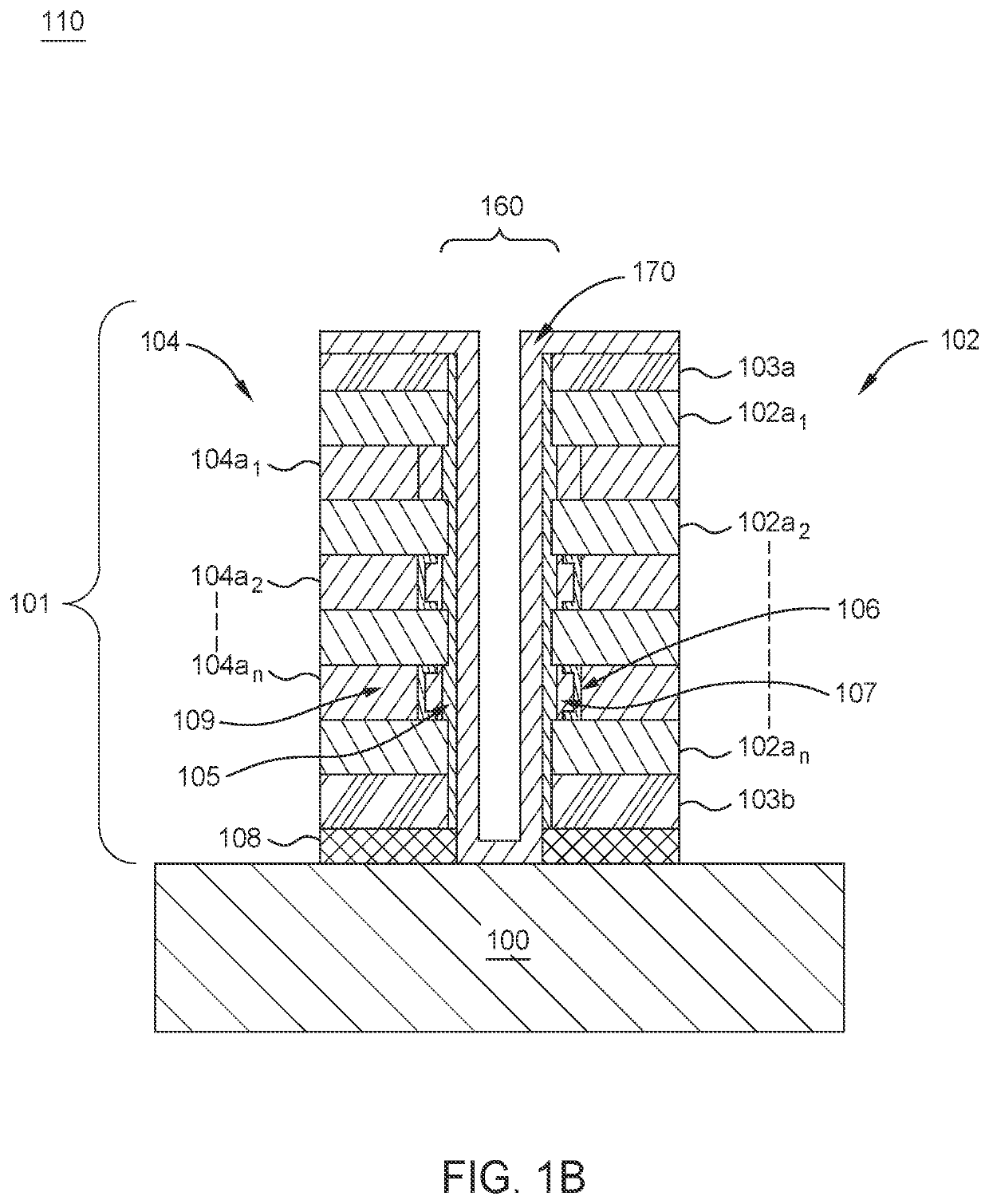
[0018]Certain aspects of the present disclosure provide systems and methods for thermally processing substrates with high aspect ratio features. In particular, high aspect ratio features can be channel structures that are formed in certain three dimensional devices. As vertical structures are created with increasingly long channel lengths, the speed of the device can become limited by the mobility of electrons in the channel and the increased lengths that the electrons must travel. Thus, there is a need to increase the mobility of electrons in the semiconductor channel in order to compensate for the increasing length that the electrons must travel. In particular, increasing grain sizes of the semiconductor, such as silicon in the channel, using thermal annealing processes can help reduce electron scattering at semiconductor grain boundaries and therefore increase mobility of electrons.

[0019]Annealing creates a more crystalline structure from regions of the substrate that were previo...


PUM


Abstract

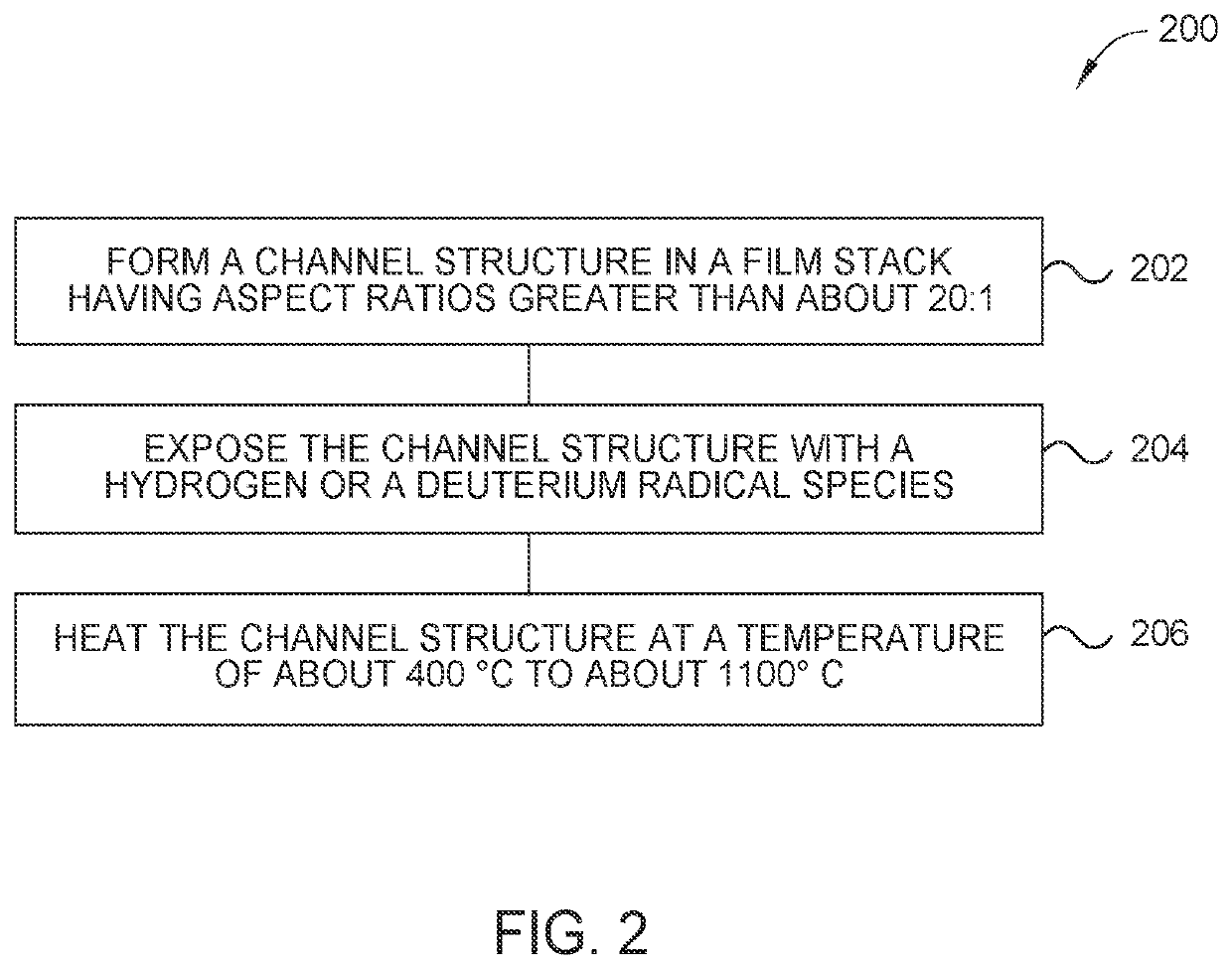
The present disclosure provides systems and methods for processing channel structures of substrates that include positioning the substrate in a first processing chamber having a first processing volume. The substrate includes a channel structure with high aspect ratio features having aspect ratios greater than about 20:1. The method includes forming a silicon-containing layer over the channel structure to a hydrogen-or-deuterium plasma in the first processing volume at a flow rate of about 10 sccm to about 5000 sccm. The substrate is maintained at a temperature of about 100° C. to about 1100° C. during the exposing, the exposing forming a nucleated substrate. Subsequent to the exposing a thermal anneal operation is performed on the substrate.

Description

CROSS-REFERENCE TO RELATED APPLICATIONS[0001]This application claims priority to U.S. Provisional Patent Application No. 62 / 986,517, dated Mar. 6, 2020, which is hereby incorporated by reference in its entirety.BACKGROUNDField[0002]Embodiments of the present disclosure generally relate to systems and methods of manufacturing a semiconductor device. More particularly, the present disclosure is directed to systems and methods of thermally processing channel structures in semiconductor devices under a hydrogen radical environment.Description of the Related Art[0003]The integrated circuit (IC) market is continually demanding greater memory capacity, faster switch speeds, and greater feature density. In order to enable fabrication of next generation devices and structures, three dimensional (3D) stacking of semiconductor memory chips are often used to improve performance of the transistors. By arranging transistors in three dimensions instead of conventional two dimensions, multiple tran...

Claims


Application Information

Patent Timeline
IPC IPC(8): H01L21/30H01L21/02
CPCH01L21/3003H01L27/11582H01L21/02667H01L21/02524H01L21/02532H01L21/02164H01L21/02252H01L21/02255H01L21/02351H01L21/0234H01L21/02236H01L21/67103H01L21/68771H10B41/27H10B43/27H01L21/02238
Inventor ZHANG, XINMINGMAYUR, ABHILASH J.SHARMA, SHASHANKTAM, NORMAN L.SPULLER, MATTHEW
Owner APPLIED MATERIALS INC
Learn More