Selective deposition of carbon on photoresist layer for lithography applications

a technology of lithography and photoresist layer, applied in the field of selective deposition of carbon on a photoresist layer, can solve the problems of inability to reliably form features with such high aspect ratio, place additional processing capabilities, unacceptable line width roughness (lwr), etc., and achieve the effect of facilitating profile and dimension control of features

Pending Publication Date: 2022-01-06
APPLIED MATERIALS INC
View PDF0 Cites 0 Cited by
  • Summary
  • Abstract
  • Description
  • Claims
  • Application Information

AI Technical Summary

Benefits of technology

[0007]Methods for forming a film stack and etching the same to form high aspect ratio features in the film stack are provided. The methods described herein facilitate profile and dimension control of features with high aspect ratios through a proper sidewall and bottom management scheme with desired materials selected for the film stack.

Problems solved by technology

However, with the continued miniaturization of circuit technology, the size and pitch of circuit features, such as interconnects, have placed additional demands on processing capabilities.
Developing film stacks and etch processes that are capable of reliably forming features with such high aspect ratios presents a significant challenge.
However, inaccurate control or low resolution of the lithography exposure and developing process may cause inaccurate dimension of a photoresist layer utilized to transfer features in a film stack, resulting in unacceptable line width roughness (LWR).
LWR and undesired wiggling profile of the photoresist layer resulting from the lithography exposure and developing process may cause inaccurate feature transfer to the film stack, eventually leading to device failure and yield loss.
Furthermore, during etching of a film stack, redeposition or build-up of by-products or other materials generated during the etching process can accumulate on the top and / or sidewalls of the features being etched, thus undesirably blocking the opening of the feature being formed in the material layer.
Furthermore, as the opening of the etched features are narrowed and / or sealed by the accumulated redeposition of material, the reactive etchants are prevented from reaching the lower surface of the features, thus limiting the aspect ratio that may be obtained.
Additionally, as the redeposition material or build-up of by-products randomly and / or irregularly adhere to the top surface and / or sidewalls of the features being etched, the resulting irregular profile and growth of the redeposition material can alter the flow path of the reactive etchants, thus resulting in bowing or twisting profiles of the features formed in the material layer.
Inaccurate profile or structural dimensions can result in collapse of the device structure, eventually leading to device failure and low product yield.
Poor etching selectivity to the materials included in the film stack can undesirably result in an inaccurate profile control, thus eventually leading to device failure.

Method used


Image

  • Selective deposition of carbon on photoresist layer for lithography applications
  • Selective deposition of carbon on photoresist layer for lithography applications
  • Selective deposition of carbon on photoresist layer for lithography applications

Examples


Embodiment Construction

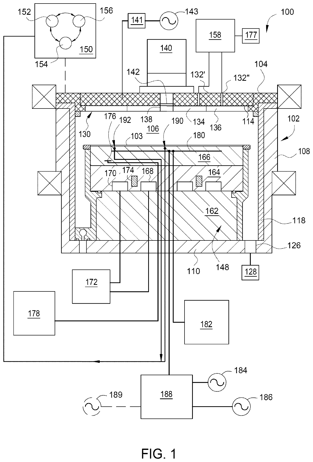
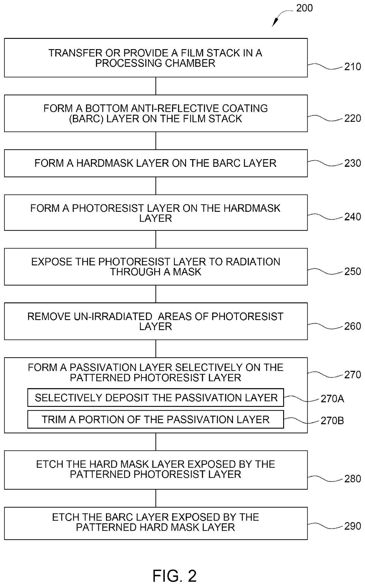
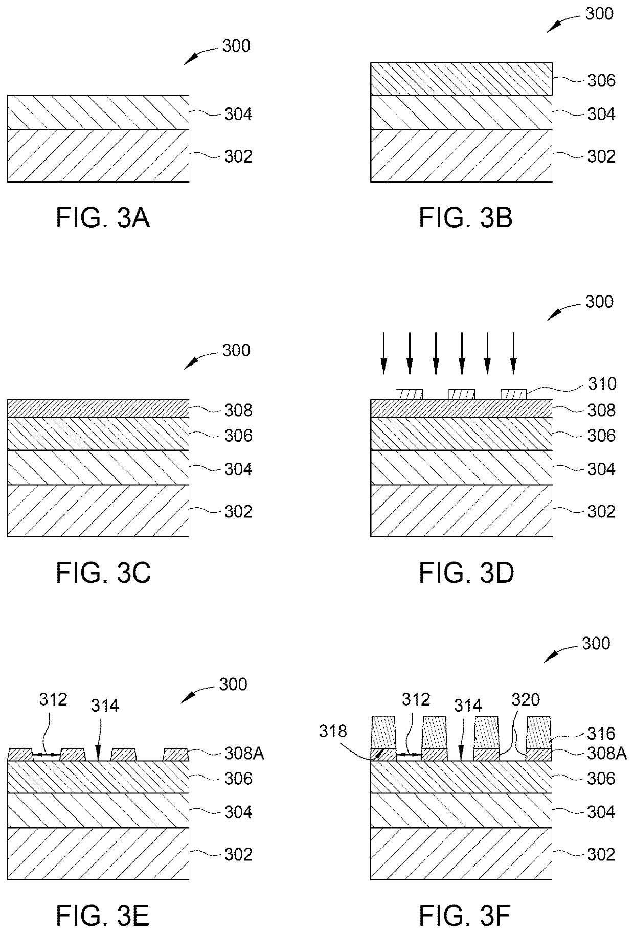
[0017]Methods for forming a film stack and etching the same to form high aspect ratio features in the film stack are provided. The methods described herein facilitate profile and dimension control of features with high aspect ratios through a proper sidewall and bottom management scheme with desired materials selected for the film stack. In particular, the methods described herein provide a metal-containing photoresist layer having a carbon-containing passivation layer selectively disposed thereon that has a high etch selectivity from an underlying metal-containing hardmask layer, leading to higher accuracy control of profile of openings etched in the hardmask layer. In addition, methods disclosed herein include methods of forming a passivation layer, including selectively depositing passivation material over a top surface of a patterned photoresist layer and trimming undesired portions of the passivation material.

[0018]As used herein, the term “about” refers to a + / −10% variation f...


PUM

PropertyMeasurementUnit
operating pressuresaaaaaaaaaa
frequencyaaaaaaaaaa
poweraaaaaaaaaa

Abstract

Embodiments disclosed within include a method for etching a hardmask layer includes forming a photoresist layer comprising an organometallic material on a hardmask layer comprising a metal-containing material, exposing the photoresist layer to ultraviolet radiation through a mask having a selected pattern, removing un-irradiated areas of the photoresist layer to pattern the photoresist layer, forming a passivation layer comprising a carbon-containing material selectively on a top surface of the patterned photoresist layer, including selectively depositing passivation material over a top surface of a patterned photoresist layer trimming undesired portions of the passivation material, and etching the hardmask layer exposed by the patterned photoresist layer having the passivation layer formed thereon.

Description

CROSS-REFERENCE TO RELATED APPLICATIONS[0001]This application claims the benefit of U.S. Provisional Patent Application Ser. No. 63 / 047,719, filed on Jul. 2, 2020, the entirety of which is herein incorporated by reference.BACKGROUNDField[0002]The embodiments herein generally relate to a method and, more specifically, to a method of selective deposition of carbon on a photoresist layer.Description of the Related Art[0003]Reliably producing submicron and smaller features is one of the key requirements of very large scale integration (VLSI) and ultra large scale integration (ULSI) of semiconductor devices. However, with the continued miniaturization of circuit technology, the size and pitch of circuit features, such as interconnects, have placed additional demands on processing capabilities. The multilevel interconnects that lie at the heart of this technology require precise imaging and placement of high aspect ratio features, such as vias and other interconnects. Reliable formation o...

Claims


Application Information

Patent Timeline
Patent Type & Authority Applications(United States)
IPC IPC(8): H01L21/027G03F7/16G03F7/20G03F7/26C23C16/26C23C16/56C23C16/04H01L21/033
CPCH01L21/0276G03F7/16G03F7/2002G03F7/26C23C16/26G03F7/0042C23C16/042H01L21/0332H01L21/0335H01L21/0337H01L21/0338C23C16/56H01L21/0273H01L21/02115H01L21/02274H01L21/31138H01L21/31116H01L21/31144H01L21/67103H01L21/67109H01L21/6831H01L21/67248G03F7/094G03F7/40
Inventor FUNG, NANCYGAO, LARRY
Owner APPLIED MATERIALS INC
Why Eureka
Try Eureka