
Method and apparatus for high aspect ratio dielectric etch

a dielectric etching and high aspect ratio technology, applied in the direction of electrolysis components, vacuum evaporation coatings, coatings, etc., can solve the problems of twisting or distortion of high aspect ratio (uhar) etching, ever-increasing aspect ratio needed to meet design requirements, etc., and achieve high aspect ratio features

Inactive Publication Date: 2013-10-10
LAM RES CORP
View PDF1 Cites 3 Cited by
  • Summary
  • Abstract
  • Description
  • Claims
  • Application Information

AI Technical Summary

Benefits of technology

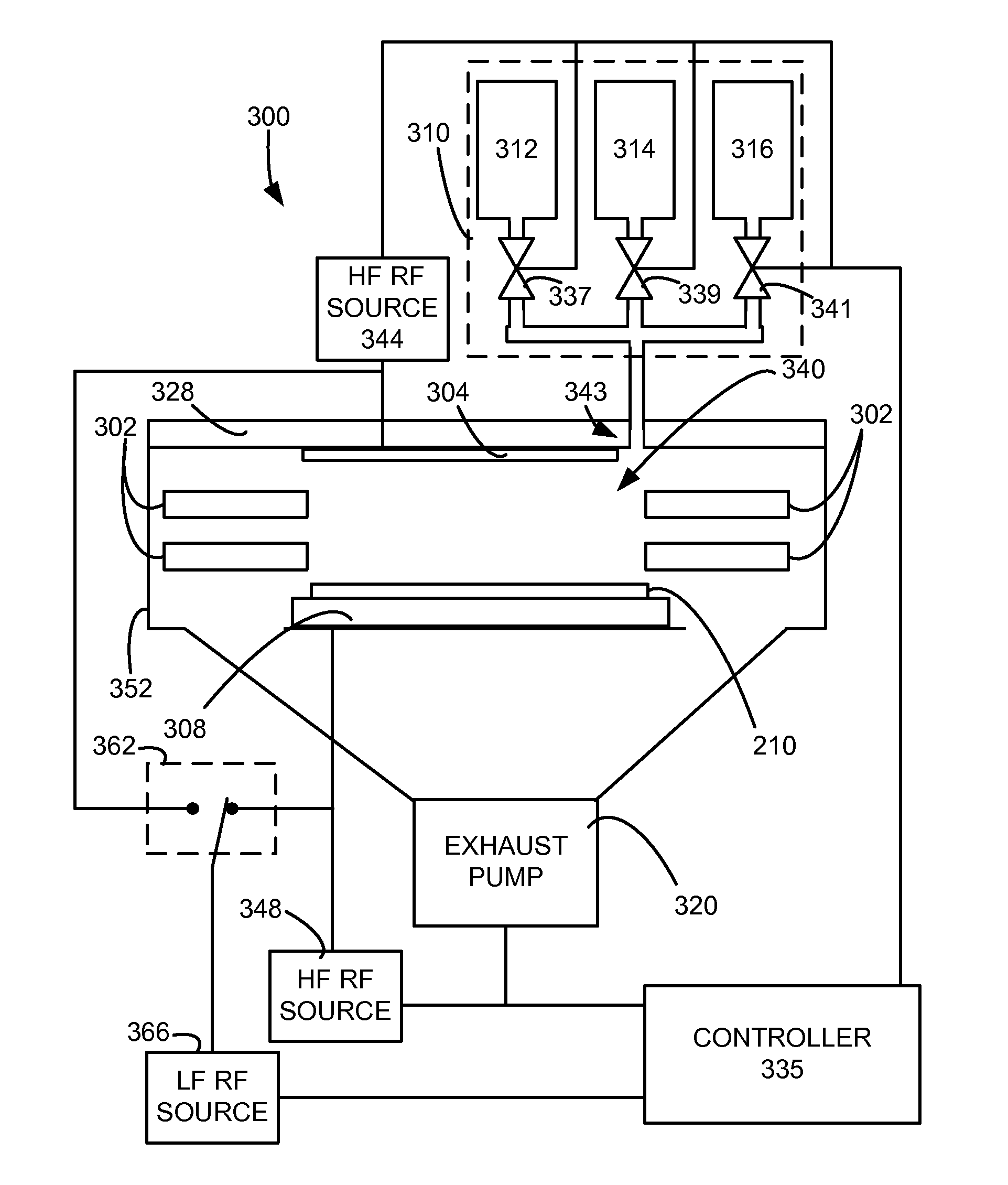
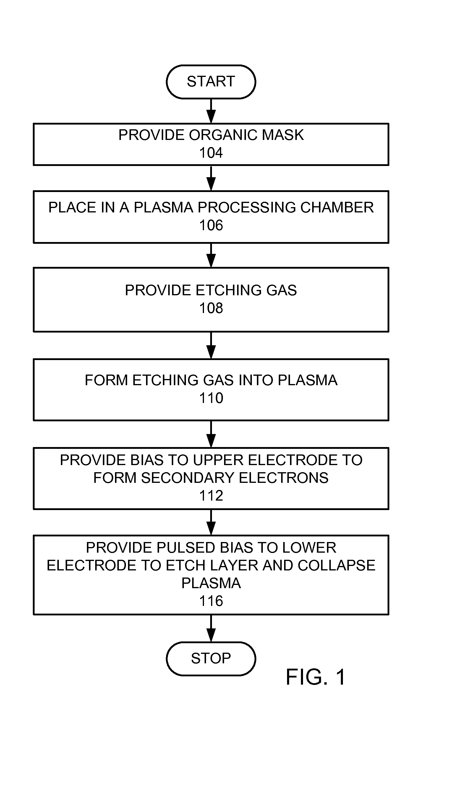
The present invention provides an apparatus and method for etching high aspect ratio features in a dielectric layer using a plasma processing chamber. The apparatus includes a chamber wall, upper and lower electrodes, a gas inlet, and a gas outlet. A high frequency RF power source is connected to the upper or lower electrodes. A bias power system is connected to both electrodes, with one bias providing secondary electrons to the upper electrode and the other providing a pulsed bias to the lower electrode to intermittently collapse a generated plasma sheath. A gas source is connected to the gas inlet, and a controller is connected to manage the gas source, high frequency RF power source, and bias power system. The method involves placing a substrate in the plasma processing chamber with the upper electrode over the substrate and the lower electrode below it. An etching gas is introduced, and a plasma is formed between the electrodes. The upper electrode is powered to form secondary electrons, while the lower electrode is pulsed to intermittently collapse the plasma sheath.

Problems solved by technology

One of the challenges faced in plasma etching is the ever-increasing aspect ratio needed to meet design requirements, especially for ultra-high density structures.
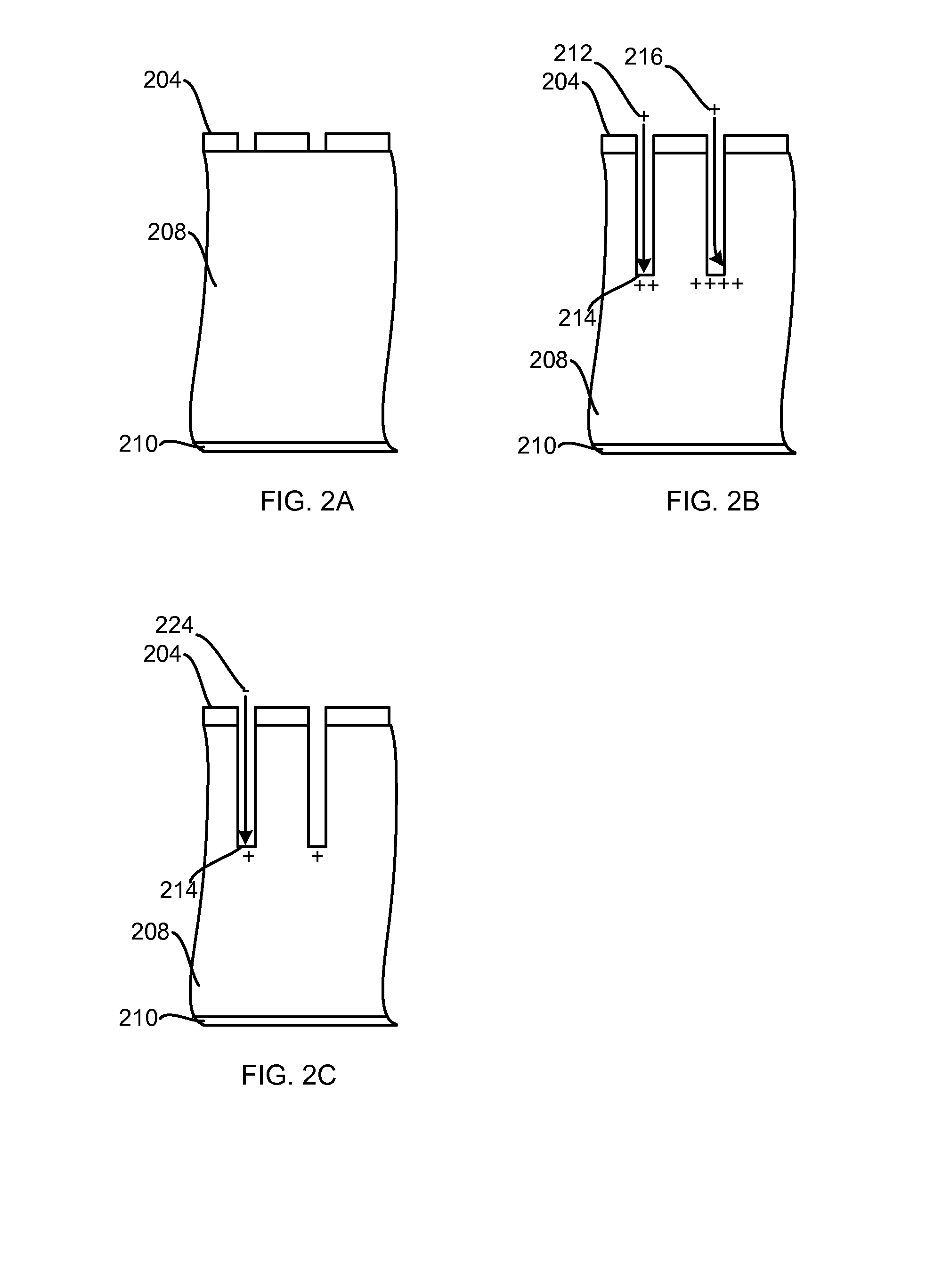
A difficulty during ultra-high aspect ratio (UHAR) etching is twisting and or distortion, which is generally defined as deviations of location, orientation, shape, and size near the bottom of a feature from the pattern defined by the mask on the top of the feature.

Method used


Image

  • Method and apparatus for high aspect ratio dielectric etch
  • Method and apparatus for high aspect ratio dielectric etch
  • Method and apparatus for high aspect ratio dielectric etch

Examples


examples

[0043]In an example of the invention, the dielectric layer may be silicon oxide based, where the dielectric layer is mainly formed of silicon oxide, with smaller amounts of other types of substance mixed in. More preferably, the dielectric layer is a low-k dielectric, such as organosilicate glass. In another embodiment the dielectric layer is an organic dielectric layer.

[0044]In an example recipe of a silicon oxide based dielectric etch, the etch chamber pressure is 30 milli-Torr (mTorr). The etch gas comprises 150 standard cubic centimeters per minute (sccm) of argon (Ar), 4 sccm of C4F6, 18 sccm of C4F8, and 17 to 25 sccm of oxygen (O2). The source HF RF power is at 2000 watts (W) with a frequency of 27 MHz. The LF RF power is 4000 W with a frequency of 2 MHz. The LF RF power is alternated between the upper and lower electrodes. The 2 Mhz power delivered to the upper and lower electrode may not be of the same magnitude and can be adjusted for optimal results.

[0045]Preferably the L...


PUM

PropertyMeasurementUnit
frequencyaaaaaaaaaa
frequencyaaaaaaaaaa
sheath voltageaaaaaaaaaa

Abstract

An apparatus for etching high aspect ratio features is provided. A plasma processing chamber is provided, comprising a chamber wall forming a plasma processing chamber enclosure, a lower electrode, an upper electrode, a gas inlet, and a gas outlet. A high frequency radio frequency (RF) power source is electrically connected to at least one of the upper electrode or lower electrode. A bias power system is electrically connected to both the upper electrode and the lower electrode, wherein the bias power system is able to provide a bias to the upper and lower electrodes with a magnitude of at least 500 volts, and wherein the bias to the lower electrode is pulsed to intermittently. A gas source is in fluid connection with the gas inlet. A controller is controllably connected to the gas source, the high frequency RF power source, and the bias power system.

Description

CROSS REFERENCE TO RELATED APPLICATIONS[0001]This application is a divisional of and claims benefit to co-pending U.S. patent application Ser. No. 12 / 429,940 filed on Apr. 24, 2009, entitled “Method and Apparatus for High Aspect Ratio Dielectric Etch,” by Edelberg, which is hereby incorporated by reference for all purposes.BACKGROUND OF THE INVENTION[0002]1. Field of the Invention[0003]The invention relates to a method of obtaining a structure on a semiconductor wafer by etching through a dielectric layer defined by a mask using a plasma.[0004]2. Description of the Related Art[0005]Plasma-etching processes are commonly used in the fabrication of semiconductor devices. Generally, photoresist material forms feature patterns on the surface of the wafer to be etched, and features are then etched into the wafer by exposing the wafer to a particular type of etching gas. One of the challenges faced in plasma etching is the ever-increasing aspect ratio needed to meet design requirements, es...

Claims


Application Information

Patent Timeline
Patent Type & Authority Applications(United States)
IPC IPC(8): H01L21/02
CPCH01J37/32091H01J37/32146H01J37/32174H01L21/02002H01J37/32449H01L21/31116H01J37/3244H01L21/3065H01L21/76825H01L21/76826
Inventor EDELBERG, ERIK A.
Owner LAM RES CORP
Learn More