Film stack for lithography applications

a technology for lithography and film stacks, applied in the direction of basic electric elements, electrical equipment, semiconductor/solid-state device manufacturing, etc., to achieve the effect of facilitating profile and dimension control of features

Active Publication Date: 2022-11-08
APPLIED MATERIALS INC
View PDF15 Cites 1 Cited by
  • Summary
  • Abstract
  • Description
  • Claims
  • Application Information

AI Technical Summary

Benefits of technology

[0007]Methods for forming a film stack and etching the same to form high aspect ratio features in the film stack are provided. The methods described herein facilitate profile and dimension control of features with high aspect ratios through a proper sidewall and bottom management scheme with desired materials selected for the film stack. In one or more embodiments, a method for etching a hardmask layer includes forming a hardmask layer on a substrate, where the hardmask layer includes a metal-containing material containing a metal element having an atomic number greater than 28, supplying an etching gas mixture to the substrate, and etching the hardmask layer exposed by a photoresist layer.

Problems solved by technology

However, with the continued miniaturization of circuit technology, the dimensions of the size and pitch of circuit features, such as interconnects, have placed additional demands on processing capabilities.
Developing a film stack and an etch processes that are capable of reliably forming features with such high aspect ratios presents a significant challenge.
However, inaccurate control or low resolution of the lithography exposure and developing process may cause in poor critical dimension of a photoresist layer utilized to transfer features in a film stack, resulting in unacceptable line width roughness (LWR).
Large line width roughness (LWR) and undesired wiggling profile of the photoresist layer resulted from the lithography exposure and developing process may cause inaccurate feature transfer to the film stack, thus, eventually leading to device failure and yield loss.
Furthermore, during etching of such film stack, redeposition or build-up of by-products or other materials generated during the etching process may accumulate on the top and / or sidewalls of the features being etched, thus undesirably blocking the opening of the feature being formed in the material layer.
Furthermore, as the opening of the etched features are narrowed and / or sealed by the accumulated redeposition of material, the reactive etchants are prevented from reaching the lower surface of the features, thus limiting the aspect ratio that may be obtained.
Additionally, as the redeposition material or build-up of by-products may randomly and / or irregularly adhere to the top surface and / or sidewalls of the features being etched, the resulting irregular profile and growth of the redeposition material may alter the flow path of the reactive etchants, thus resulting in bowing or twisting profiles of the features formed in the material layer.
In accurate profile or structural dimensions may result in collapse of the device structure, eventually leading to device failure and low product yield.
Poor etching selectivity to the materials included in the film stack may undesirably result in an inaccurate profile control, thus eventually leading to device failure.

Method used


Image

  • Film stack for lithography applications
  • Film stack for lithography applications
  • Film stack for lithography applications

Examples


Embodiment Construction

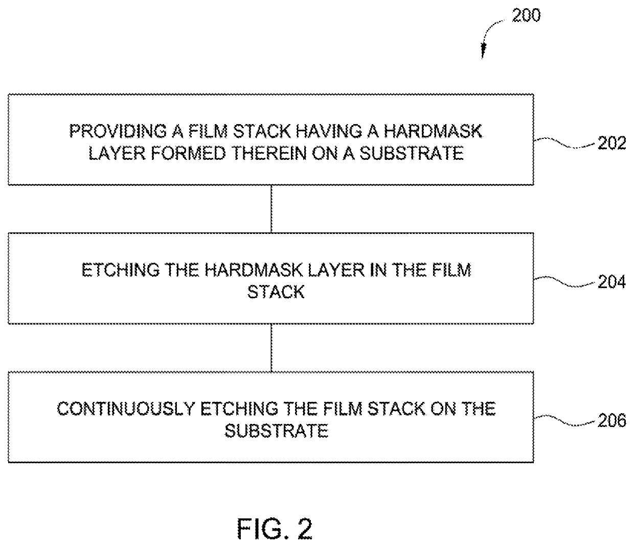
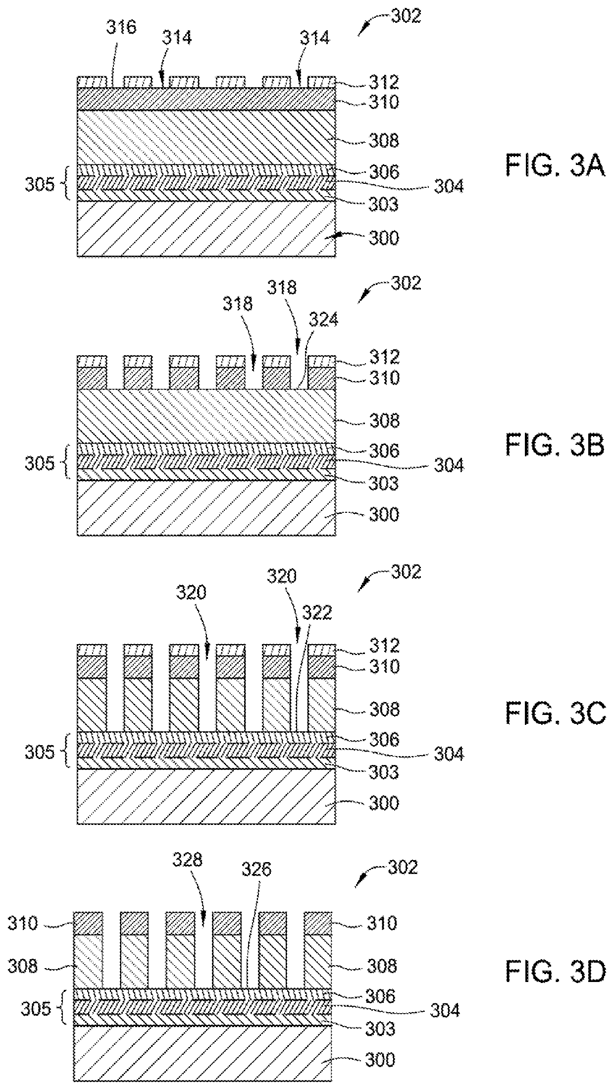
[0019]Embodiments for the present application includes methods for forming a film stack and an etching process to etch such film stack to form features having desired aspect ratios and profiles in the film stack. The film stack includes a hardmask layer having a metal-containing material in the film stack. The hardmask layer may be a single layer or multiple layers with selected film properties to assist etching resistance and enhance lithography exposure performance as needed. In one or more embodiments, the hardmask layer is a metal-containing material with desired absorption coefficient or mixture of different values of absorption coefficient so as to assist the exposure and developing accuracy during the lithography exposure process. An etching process with desired chemistry is also selected to pattern the film stack, particularly to etch the hardmask layer.

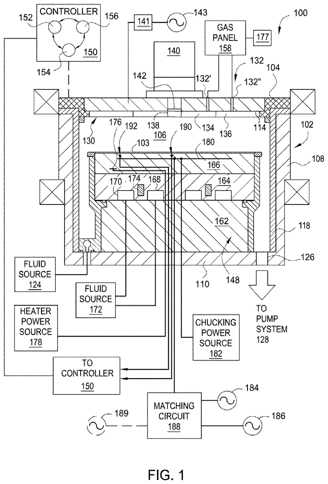
[0020]FIG. 1 is a sectional view of one example of a processing chamber 100 suitable for performing a patterning process to...


PUM

PropertyMeasurementUnit
atomic numberaaaaaaaaaa
operating pressuresaaaaaaaaaa
frequencyaaaaaaaaaa

Abstract

Methods for forming a film stack comprising a hardmask layer and etching such hardmask layer to form features in the film stack are provided. The methods described herein facilitate profile and dimension control of features through a proper profile management scheme formed in the film stack. In one or more embodiments, a method for etching a hardmask layer includes forming a hardmask layer on a substrate, where the hardmask layer contains a metal-containing material containing a metal element having an atomic number greater than 28, supplying an etching gas mixture to the substrate, and etching the hardmask layer exposed by a photoresist layer.

Description

CROSS-REFERENCE TO RELATED APPLICATIONS[0001]This application claims benefit of U.S. Appl. No. 62 / 810,133, filed Feb. 25, 2019, which is incorporated by reference in its entirety.BACKGROUNDField[0002]The embodiments herein generally relate to a film stack and an etching process for etching such film stack with high selectivity and good profile control to EUV lithography exposure and patterning process.Description of the Related Art[0003]Reliably producing submicron and smaller features is one of the key requirements of very large scale integration (VLSI) and ultra large scale integration (ULSI) of semiconductor devices. However, with the continued miniaturization of circuit technology, the dimensions of the size and pitch of circuit features, such as interconnects, have placed additional demands on processing capabilities. The multilevel interconnects that lie at the heart of this technology require precise imaging and placement of high aspect ratio features, such as vias and other ...

Claims


Application Information

Patent Timeline
Patent Type & Authority Patents(United States)
IPC IPC(8): H01L21/033H01L21/311
CPCH01L21/0337H01L21/0332H01L21/31116H01L21/31122H01L21/31144H01L21/32136
Inventor SINGH, TEJINDERPARIKH, SUKETU ARUNDIEHL, DANIEL LEESTOLFI, MICHAEL ANTHONYRAMALINGAM, JOTHILINGAMCAO, YONGYAN, LIFANLANG, CHI-IHWANG, HOYUNG DAVID
Owner APPLIED MATERIALS INC
Why Eureka
Try Eureka