Donor-acceptor interfaces for excitonic semiconductors

a semiconductor and donor technology, applied in semiconductor devices, solid-state devices, light-sensitive devices, etc., can solve the problems of reducing the overall photocurrent generation efficiency and the “bulky” organic cation, and achieve the effect of low exciton binding energy, efficient exciton dissociation, and notable progress in solar cell power conversion efficiency (pce)

Pending Publication Date: 2021-09-23
THE TRUSTEES FOR PRINCETON UNIV
View PDF0 Cites 2 Cited by
  • Summary
  • Abstract
  • Description
  • Claims
  • Application Information

AI Technical Summary

Benefits of technology

[0010]Three-dimensional (3D) hybrid organic-inorganic metal halide perovskite semiconductors (e.g., CH3NH3PbI3 or MAPbI3), which have achieved notable progress in solar cell power conversion efficiency (PCE) in recent years, possess low exciton binding energies and therefore do not require donor-acceptor structures to produce photocurrent. In contrast, lower-dimensional perovskite semiconductors including two-dimensional (2D) perovskites such as Ruddlesden-Popper phases or Dion-Jacobson phases may utilize donor-acceptor heterojunctions for efficient exciton dissociation. In certain applications, 2D perovskites are more desirable than 3D perovskites due to improved moisture and thermal stability.

Problems solved by technology

As noted above, larger exciton binding energies reduce overall photocurrent generation efficiency.
In this case, an organic cation may be considered to be “bulky” if it is large enough so that it cannot fit into the 3D metal halide perovskite lattice.

Method used


Image

  • Donor-acceptor interfaces for excitonic semiconductors
  • Donor-acceptor interfaces for excitonic semiconductors
  • Donor-acceptor interfaces for excitonic semiconductors

Examples


Embodiment Construction

[0046]The following is a detailed description of certain embodiments chosen to provide illustrative examples of how the disclosed invention may preferably be implemented. The scope of the disclosed invention is not limited to the specific embodiments described herein.

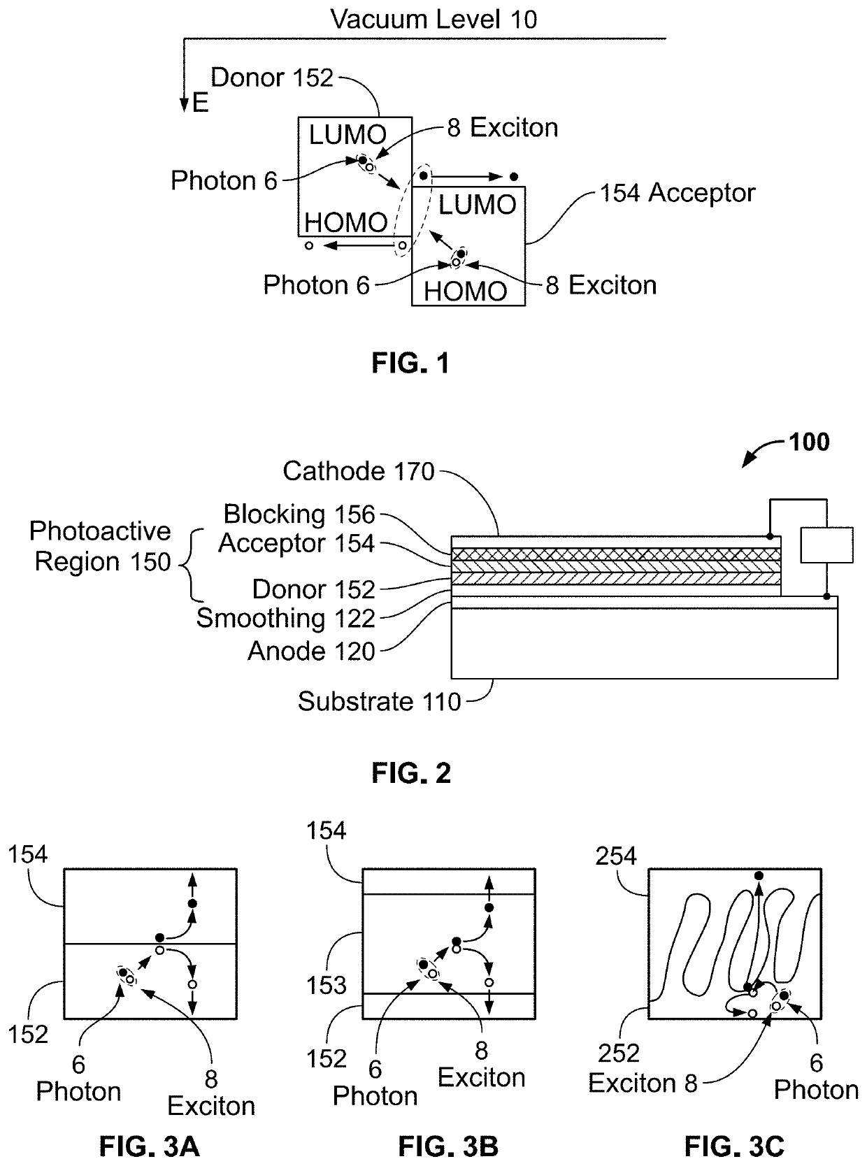
[0047]FIG. 2 is a block diagram illustrating an example of an organic photosensitive optoelectronic device 100 according to one embodiment, in which the photoactive region 150 comprises a donor-acceptor heterojunction. The “photoactive region” is a portion of the photosensitive device that absorbs electromagnetic radiation to generate excitons that may dissociate in order to generate an electrical current. Generally, excitons may be created and be stable in a material when the excitonic binding energy of the material is greater than 1-3 times the thermal energy of the material. The thermal energy is represented by kT, wherein k represents the Boltzmann constant and T represents temperature. In contrast, if the excitonic...


PUM

PropertyMeasurementUnit
LUMOaaaaaaaaaa
exciton binding energiesaaaaaaaaaa
exciton binding energyaaaaaaaaaa

Abstract

Provided is a thin film semiconductor device that exploits excitonic characteristics of various organic semiconductor materials. The device may include an anode (120), a cathode (170), and a donor-acceptor heterojunction (150) disposed between the anode and the cathode. The donor-acceptor heterojunction may further include an acceptor material (404) having a highest occupied molecular orbital (HOMO) and a lowest unoccupied molecular orbital (LUMO), and a donor material (402) comprising a hybrid organic-inorganic metal halide perovskite semiconductor. Other embodiments are disclosed and additional embodiments are also possible.

Description

CROSS-REFERENCE TO RELATED APPLICATION(S)[0001]This application is based on and claims priority to U.S. Provisional Application No. 62 / 719,977, filed on Aug. 20, 2018, the disclosure of which, including the appendix, is incorporated by reference herein its entirety.UNITED STATES GOVERNMENT RIGHTS[0002]This invention was made with government support under Grant No. N00014-17-1-2005 awarded by the Office of Naval Research and Grant No. DE-SC0012458 awarded by the Department of Energy. The government has certain rights in the invention.BACKGROUNDTechnical Field[0003]The instant disclosure generally relates to thin film semiconductor devices. More specifically, in one or more embodiments, it is directed to organic photosensitive optoelectronic devices having donor-acceptor heterojunctions where the donor material is a hybrid organic-inorganic metal halide perovskite semiconductor that includes bulky ligands, and the acceptor is an organic semiconductor.Background Art[0004]Optoelectronic...

Claims


Application Information

Patent Timeline
Patent Type & Authority Applications(United States)
IPC IPC(8): H01L51/42H01G9/20H01L51/00
CPCH01L51/426H01L51/4213H01G9/20H01L51/0026H01L51/0003H01L51/001H01L51/0077Y02E10/549H10K30/20H10K85/50H10K30/35H10K30/10H10K85/30H10K71/12H10K71/40H10K71/164
Inventor RAND, BARRY P.ZHAO, LIANFENG
Owner THE TRUSTEES FOR PRINCETON UNIV
Why Eureka
Try Eureka