Transistor structure and related inverter
a transistor and inverter technology, applied in the direction of transistors, electrical devices, semiconductor devices, etc., can solve the problems of reducing the complexity of the multiple layers of interconnection, and achieve the effects of enhancing the speed performance of the cmos circuit, reducing power and die area, and increasing the immunity to nois
- Summary
- Abstract
- Description
- Claims
- Application Information
AI Technical Summary
Benefits of technology
Problems solved by technology
Method used
Image

Examples
first embodiment
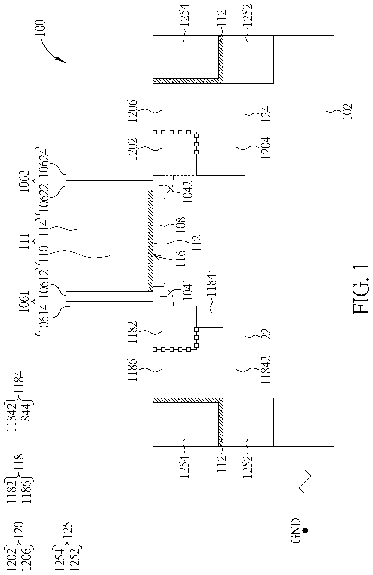
[0054]Please refer to FIG. 1. FIG. 1 is a diagram illustrating a cross section of an NMOS transistor 100 according to the present invention. As shown in FIG. 1, the NMOS transistor 100 includes a p-type substrate 102, spacers 1061, 1062, a channel region 108, a gate structure 111, a first conductive region 118, a second conductive region 120, and a trench isolation layer 125 (that is, a deep shallow trench isolation structure), wherein the p-type substrate 102 can be a silicon substrate or III-V group substrate, the NMOS transistor 100 can be a tri-gate transistor, FinFET (fin field-Effect transistor), GAA (Gate-All-Around) FET, fin-structure transistor, or other type transistor, and the p-type substrate 102 could be connected to ground GND. In addition, the spacer 1061 includes an oxide-1 spacer layer 10612, and a Nitride-1 spacer layer 10614, and the spacer 1062 includes an oxide-1 spacer layer 10622, and a Nitride-1 spacer layer 10624. But, the spacers 1061, 1062 are not limited ...
third embodiment
[0102]Please refer to FIG. 9. FIG. 9 is a diagram illustrating a structure of an NMOS transistor 900 in a CMOS inverter according to the present invention. As shown in FIG. 9, a difference between the NMOS transistor 900 and the NMOS transistor 100 is that a first guard isolation layer 902 close to a CMM (or a CMC) 904 (i.e. the first metal containing region 1186 shown in the NMOS transistor 100) only includes a vertical guard isolation portion but without a horizontal guard isolation portion. The vertical guard isolation portion contacts to the bottom of the first semiconductor region 1182 and a sidewall of the CMM 904, and the CMM 904 directly contacts to the p-type substrate 102. Since both the CMM 904 and the p-type substrate 102 of the NMOS transistor 900 are connected to the ground GND (0 V electrical potential), the CMM 904 does not have a barrier of the first guard isolation layer 902 so as to make the CMM 904 directly electrically contact to the p-type substrate 102 which i...
fourth embodiment
[0105]Please refer to FIG. 11. FIG. 11 is a diagram illustrating a cross-section of a CMOS inverter 1100 according to the present invention, wherein the CMOS inverter 1100 includes an NMOS transistor 1102 and a PMOS transistor 1104, a structure of the NMOS transistor 1102 can be referred to the NMOS transistor 900 shown in FIG. 9, and a structure of the PMOS transistor 1104 can be referred to the PMOS transistor 1000 shown in FIG. 10. As shown in FIG. 11, a first conductive region of the NMOS transistor 1102 is formed in a first concave 1150, a second conductive region of the NMOS transistor 1102 is formed in a second concave 1160, a third conductive region of the PMOS transistor 1104 is formed in the first concave 1150, and a fourth conductive region of the PMOS transistor 1104 is formed in a third concave 1170, wherein a first metal containing region included in the first conductive region of the NMOS transistor 1102 is electrically coupled to a first heavily doped n-type semicond...
PUM
 Abstract
Description
Claims
Application Information
 - R&D Engineer
- R&D Manager
- IP Professional
- Industry Leading Data Capabilities
- Powerful AI technology
- Patent DNA Extraction
Browse by: Latest US Patents, China's latest patents, Technical Efficacy Thesaurus, Application Domain, Technology Topic.
© 2024 PatSnap. All rights reserved.Legal|Privacy policy|Modern Slavery Act Transparency Statement|Sitemap