Novel High Speed High Density NAND-Based 2T-NOR Flash Memory Design

a flash memory and high density technology, applied in the field of design of two transistor nor (2tnor) flash memory, can solve the problems of limiting the use of the cell in ultra high integrated levels of flash memory below 0.18 um technology, the channel length of the cell is very difficult to be scaled down, and the physical limitation of how small the cell, etc., to achieve the effect of simplifying the design of the on-chip state machine, high driving capability and high speed

Inactive Publication Date: 2011-06-30
APLUS FLASH TECH
View PDF3 Cites 18 Cited by
  • Summary
  • Abstract
  • Description
  • Claims
  • Application Information

AI Technical Summary

Benefits of technology

[0016]The read-row-decoder of the present invention is made of a medium-high voltage device for the boosted voltage to operate at around 4.0V during fast random reading. There are two high voltage (HV) enhancement NMOS devices for isolation between the write-row-decoder and read-row-decoder for the access transistors. Both HV NMOS devices separate the write-row-decoder and the read-row-decoder. The capability of coupling voltage from the triple P-well of the flash cell can be obtained by turning off those two HV NMOS devices during erasing. By using the read-row-decoder through the isolation HV NMOS device to connect the select gates of access transistors, high driving capability is provided to achieve high speed requirement in some embedded applications.
[0017]The invention uses the access transistor to overcome the over-erase issue commonly seen in the 1T-NOR flash memory. It simplifies the design of the on-chip state machine. A preferred voltage for the unselected word lines is provided for a channel program operation so that the disturbance of the Vt of the unselected cells can be eliminated or substantially reduced. In addition, the invention uses 3-state MLC design for high speed applications during reading. A fixed preferred word line (WL) voltage level and a low enough memory cell Vt provide high enough cell current. It offers ultra-high density, low cost and high speed solution for the flash memory in embedded applications.
[0018]For high speed embedded applications, the present invention offers two approaches to enhancing the memory cell current during reading. For applications requiring low power, the first approach applies Vdd (1.8V or 3V) level to all the storage transistors. Therefore, there is no need of boosted WL due to the relatively high enough cell current with the negative Vt for the erased-state storage device. However, there is always a need of boosted voltage, e.g. 4V, for the access device because its Vt is around 0.75V. The second approach replaces Vdd level by the boosted voltage. Compared to the first approach, the latter one has the lowest resistance while reading. It provides high speed performance with relatively high power because the gate voltage of both storage device and access device comes from the same boosted voltage source.

Problems solved by technology

Due to this CHE scheme, the cell's channel length is very difficult to be scaled down.
This causes a physical limitation on how small the cell can be made and in turn limits the use of the cell in ultra high integrated levels of the flash memory below 0.18 um technology.
Furthermore, the negative FN-edge programming causes device oxide degradation because the electron-hole pairs at the biased drain to triple P-well (TPW) junction are accelerated by the voltage difference between the drain and the source.
However, the drain induced leakage current may occur if the channel length is scaled down in the cell.
Therefore, the flash memory still encounters the scaling issue and ends up with a large memory cell size.
The channel length of the access device can not be shortened because of the drain induced leakage current to the common source line when the program inhibit voltage is applied across the drain and the source.

Method used


Image

  • Novel High Speed High Density NAND-Based 2T-NOR Flash Memory Design
  • Novel High Speed High Density NAND-Based 2T-NOR Flash Memory Design
  • Novel High Speed High Density NAND-Based 2T-NOR Flash Memory Design

Examples


first embodiment

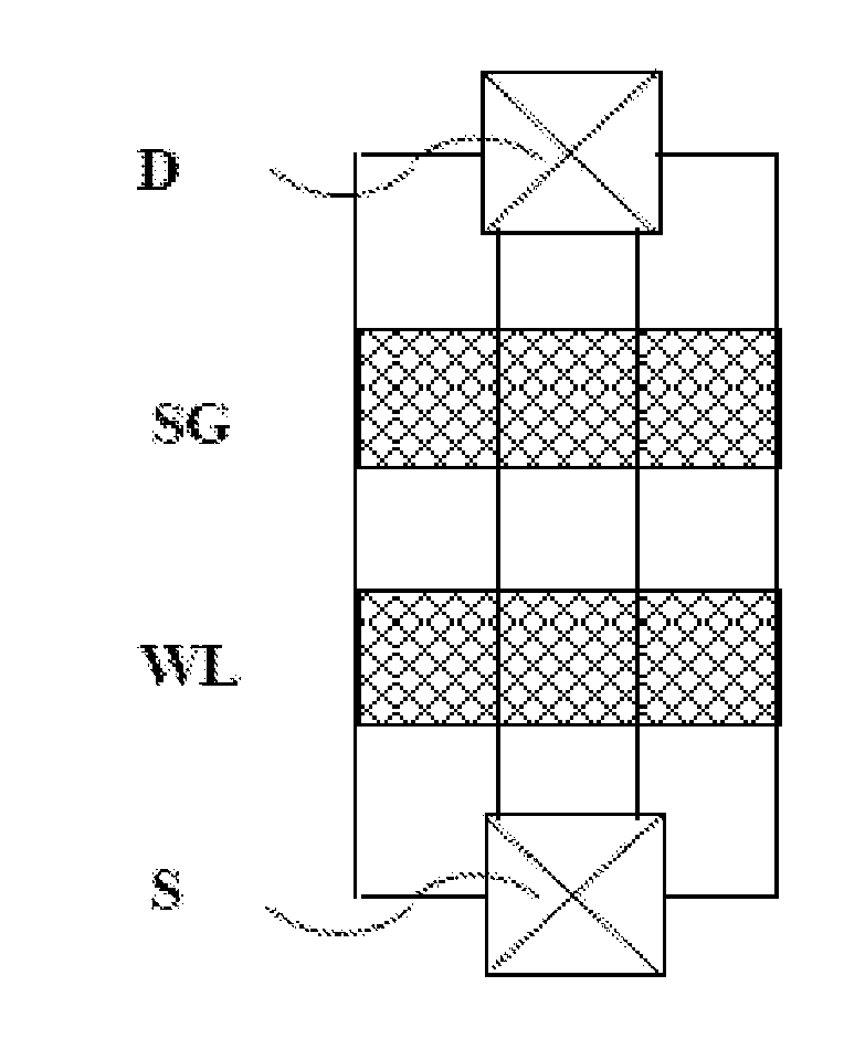
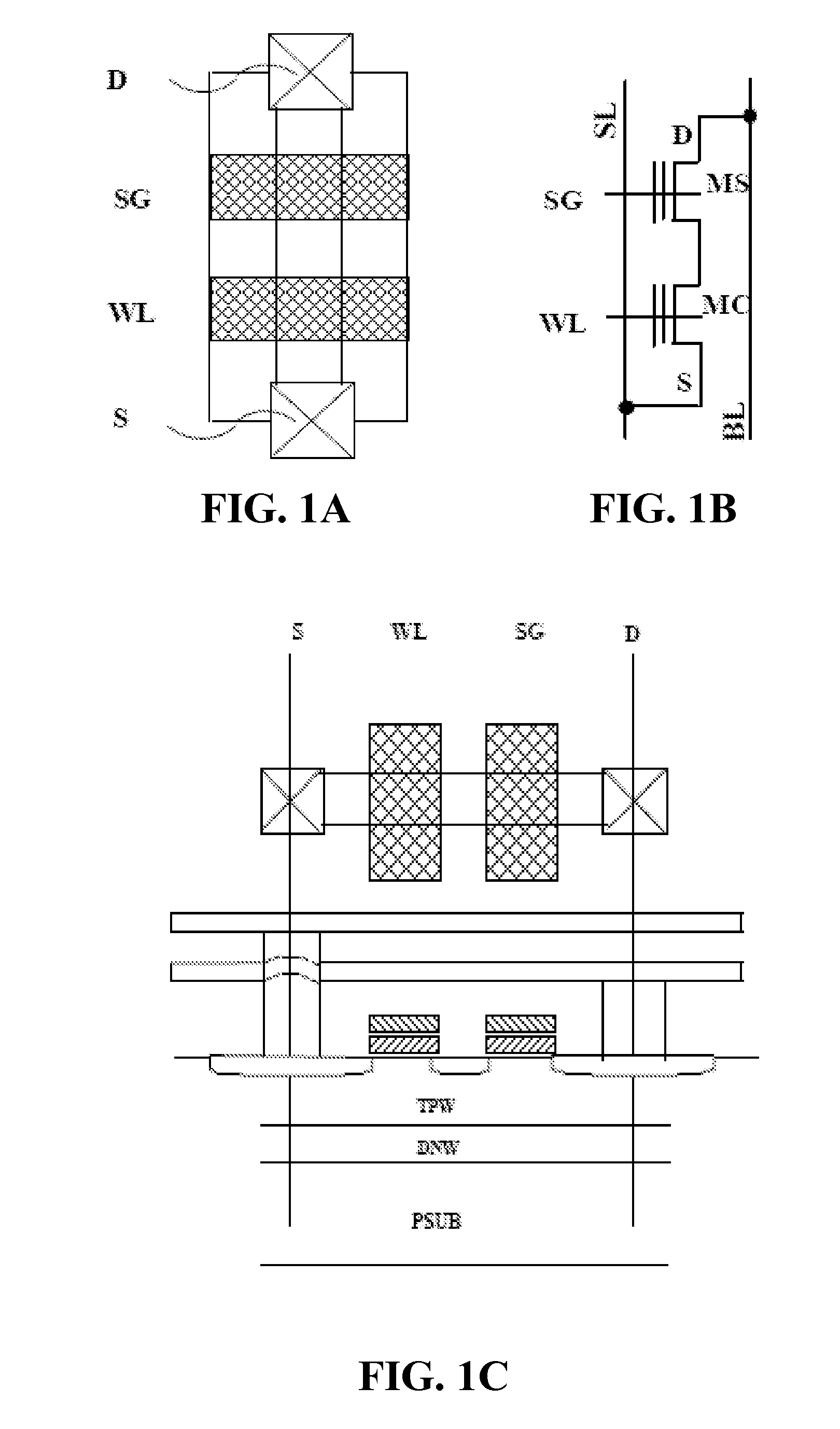
[0054]FIG. 1A is a top view of the plan layout of a floating-gate type NMOS, NAND-based 2T-NOR flash cell of the first embodiment in the present invention. The figure only shows four key connection nodes of the drain (N-active), source (N-active), select gate for accessing the device, and the cell gate of the storage device in the flash cell and they are denoted as D, S, SG and WL respectively. The S node has a half contact for a source line connection and the D node has a half for a bit line connection.

[0055]FIG. 1B shows a schematic diagram for the circuit of the NAND-based 2T-NOR flash cell according to FIG. 1A of the present invention. The access transistor MS and the storage transistor MC are both made of a 2-poly floating-gate cell. The circuit of the 2T-NOR flash cell has four terminals for D, SG, WL and S. The D node is connected to a local vertical metal bit line denoted as BL and the S node is connected to a local vertical metal source line denoted as SL. In contrast to th...

second embodiment

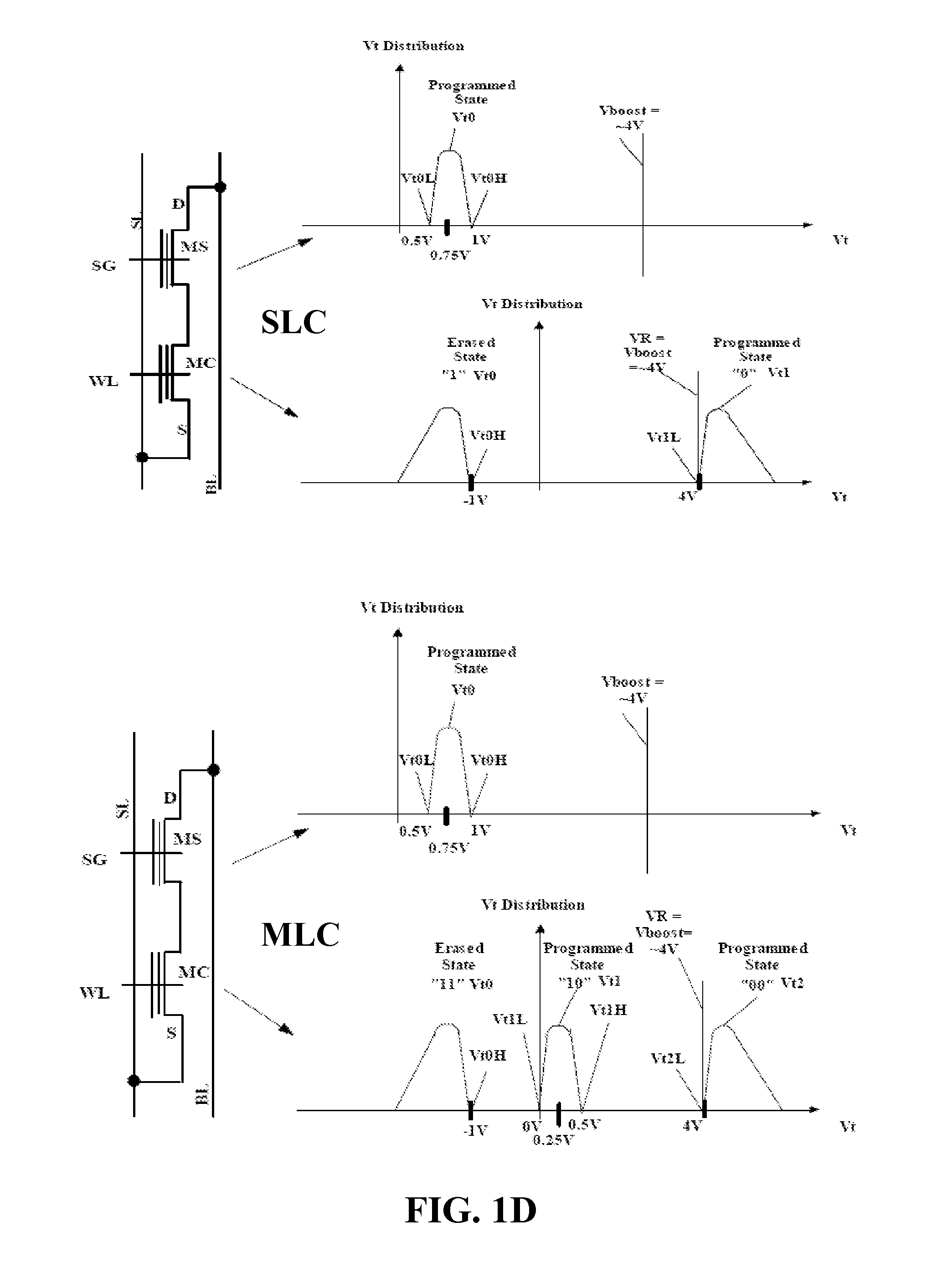
[0061]FIG. 2 shows the circuit diagram of a NAND-based 2T-NOR flash cell according to the present invention and the threshold voltage distributions of the corresponding SLC and MLC. In this embodiment, the storage transistor MC is a 2-poly floating-gate NAND cell while the access transistor MS is a poly1 transistor made of a double poly NMOS device with poly1 and poly2 shorted and strapped to form an access line to connect a row of access transistors. For the access transistor MS, the threshold voltage Vt is the threshold voltage of the poly1 NMOS transistor. This Vt0 is set with a preferred center value of +0.75V, ranging from +0.5V to +1V in accordance with the present invention.

[0062]For the storage transistor MC, the Vt distribution of two state SLC shows the erased state (0H=−1V) and the programmed state (>Vt1L=4V). The Vt ranges of both states can be widely spread without concern of over-erase or over-program. The Vt distribution of the three state MLC in FIG. 2 shows the eras...

third embodiment

[0063]FIG. 3A is a top view of the plan layout of a floating-gate type NMOS, NAND-based 2T-NOR flash cell of the third embodiment in the present invention. Only four key connection nodes of drain (N-active), source (N-active), select gate for accessing the device, and the cell gate of the storage device are shown and they are denoted as D, S, SG and WL respectively. The S node has a half contact for a source line connection and the D node has a half for a bit line connection.

[0064]FIG. 3B shows a schematic diagram for the circuit of the NAND-based 2T-NOR flash cell according to FIG. 3A of the present invention. The access transistor MS is made of an either poly1 or poly2 NMOS device dependent on which manufacturing process is appropriate for application. The flash storage transistor MC is still made of a 2-poly floating-gate cell. The circuit of the 2T-NOR flash cell has four terminals for D, SG, WL and S. The D node is connected to a local vertical metal bit line denoted as BL and ...


PUM


Abstract

A two transistor NOR flash memory cell has symmetrical source and drain structure manufactured by a NAND-based manufacturing process. The flash cell comprises a storage transistor made of a double-poly NMOS floating gate transistor and an access transistor made of a double-poly NMOS floating gate transistor, a poly1 NMOS transistor with poly1 and poly2 being shorted or a single-poly poly1 or poly2 NMOS transistor. The flash cell is programmed and erased by using a Fowler-Nordheim channel tunneling scheme. A NAND-based flash memory device includes an array of the flash cells arranged with parallel bit lines and source lines that are perpendicular to word lines. Write-row-decoder and read-row-decoder are designed for the flash memory device to provide appropriate voltages for the flash memory array in pre-program with verify, erase with verify, program and read operations in the unit of page, block, sector or chip.

Description

[0001]This application claims the benefit of priority to U.S. Provisional Patent Application Ser. No. 61 / 270,583, filed Jul. 10, 2009, which is incorporated herein by reference in its entirety.CROSS REFERENCES TO RELATED APPLICATIONS[0002]This application is related to U.S. patent application Ser. No. 12 / 387,771, filed on May 7, 2009 and Ser. No. 12 / 455,936, filed on Jun. 9, 2009, assigned to the same assignee as the present invention, and incorporated herein by reference in the entirety.FIELD OF THE INVENTION[0003]This invention relates generally to a single-chip low-voltage and high read speed nonvolatile memory (NVM), and more specifically to the design of a two transistor NOR (2T-NOR) flash memory by using NAND-based cell structure, cell operation schemes and manufacturing process.BACKGROUND OF THE INVENTION[0004]Nonvolatile memory is well known in the art. The different types of nonvolatile memory include read-only-memory (ROM), electrically programmable read only memory (EPROM...

Claims


Application Information

Patent Timeline
Patent Type & Authority Applications(United States)
IPC IPC(8): G11C16/04
CPCG11C16/0425G11C16/10H01L27/11521H01L27/11519H10B41/10H10B41/30G11C16/02G11C16/06
Inventor LEE, PETER WUNGHSU, FU-CHANG
Owner APLUS FLASH TECH
Why Eureka
Try Eureka