Supercharge Your Innovation With Domain-Expert AI Agents!

Process and structure of overlay offset measurement

a technology of offset measurement and process, applied in the direction of instruments, photomechanical equipment, radio frequency control devices, etc., can solve the problem that the offset (or shift) measurement cannot be properly performed while manufacturing the electronic device, and achieve the effect of facilitating the offset measuremen

Active Publication Date: 2021-11-18
HIMAX TECH LTD
View PDF1 Cites 0 Cited by
  • Summary
  • Abstract
  • Description
  • Claims
  • Application Information

AI Technical Summary

Benefits of technology

The present invention aims to provide a semiconductor structure and process that facilitate the measurement of overlay offset. This refers to the alignment of different components in a semiconductor device. The technical effect of this invention is to improve the accuracy and reliability of semiconductor device manufacturing.

Problems solved by technology

However, as a layer of an electronic device, such as optoelectronic device, may have a thickness so large (e.g., greater than 14 μm) that overlay offset (or shift) measurement cannot be properly performed while manufacturing the electronic device.

Method used


Image

  • Process and structure of overlay offset measurement
  • Process and structure of overlay offset measurement

Examples


Embodiment Construction

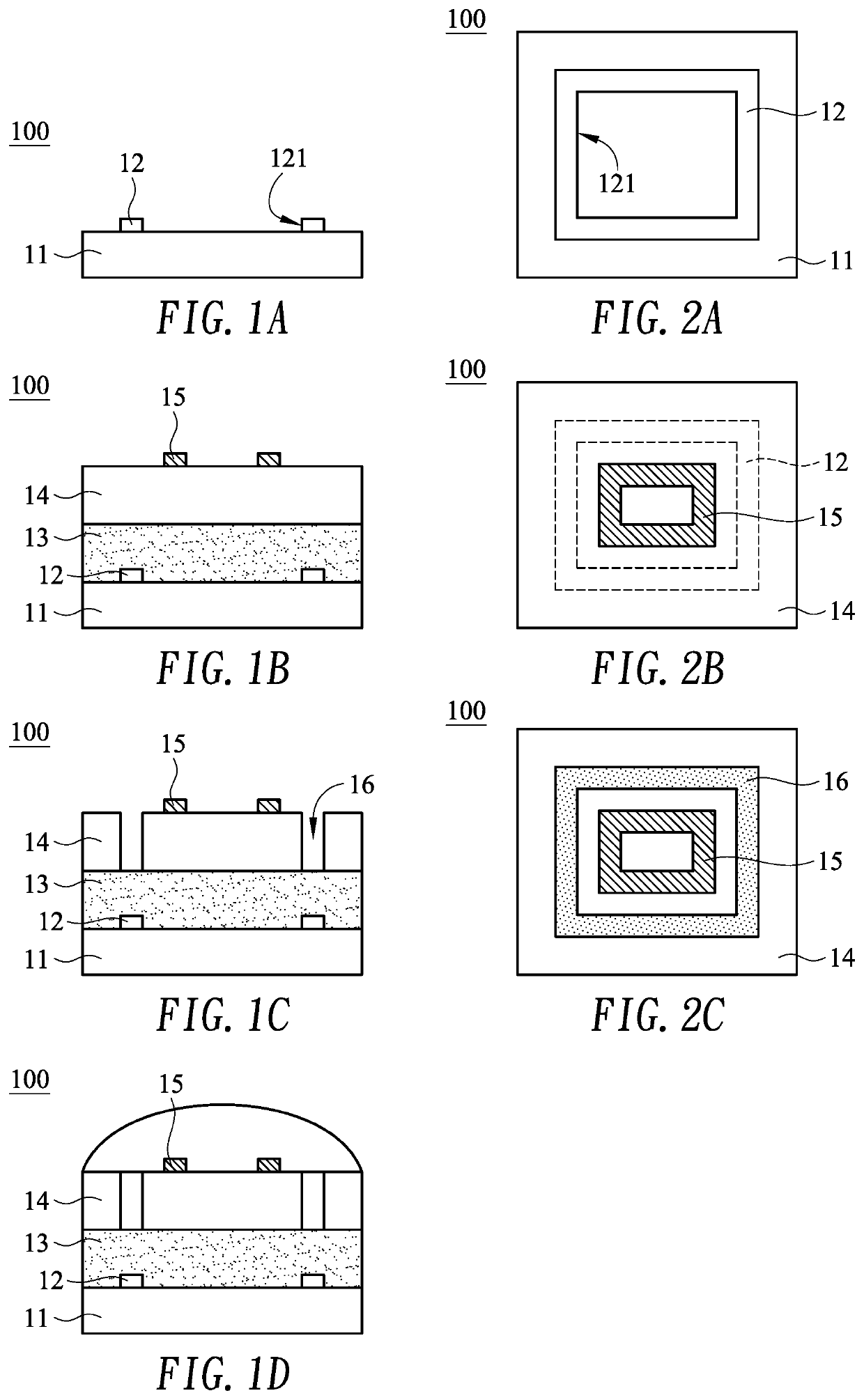
[0010]FIG. 1A to FIG. 1D show cross-sectional views (e.g., on a cutting line or path) illustrating a semiconductor process that facilitates overlay offset (or shift or error) measurement while manufacturing an electronic device 100 according to one embodiment of the present invention, and FIG. 2A to FIG. 2C show corresponding top views of FIG. 1A to FIG. 1C. Although an optoelectronic device, such as fingerprint sensor, is exemplified in the embodiment, it is appreciated that the embodiment may be generally adaptable to an electronic device that requires overlay offset measurement to be performed while manufacturing the electronic device.

[0011]Referring to FIG. 1A (cross-sectional view) and FIG. 2A (top view), a substrate (e.g., semiconductor wafer or glass) 11 is provided. Next, a first pattern layer 12 with a predetermined first pattern acting as a mark is formed on the substrate 11. In the embodiment, the first pattern layer 12 includes a first frame (i.e., the first pattern) hav...


PUM

PropertyMeasurementUnit
thicknessaaaaaaaaaa
thicknessaaaaaaaaaa
structureaaaaaaaaaa

Abstract

A process of overlay offset measurement includes providing a substrate; forming a first pattern layer with a predetermined first pattern on the substrate; forming a first photoresist layer on the substrate and the first pattern layer; forming a second photoresist layer on the first photoresist layer; forming a second pattern layer with a predetermined second pattern on the second photoresist layer; patterning the second photoresist layer to form a trench having a predetermined third pattern being substantially aligned with the predetermined first pattern of the first pattern layer; and performing overlay offset measurement according to the second pattern layer and the trench.

Description

BACKGROUND OF THE INVENTION1. Field of the Invention[0001]The present invention generally relates to overlay offset measurement, and more particularly to a semiconductor structure and process that facilitate overlay offset measurement.2. Description of Related Art[0002]As the critical dimension of a semiconductor device progressively decreases due to advancing technology, the tolerance to offset between layers becomes lower. The alignment or overlay measurement between layers may be measured by overlay measure tools.[0003]However, as a layer of an electronic device, such as optoelectronic device, may have a thickness so large (e.g., greater than 14 μm) that overlay offset (or shift) measurement cannot be properly performed while manufacturing the electronic device.[0004]A need has thus arisen to propose a novel scheme to overcome the drawbacks of overlay offset measurement while manufacturing the electronic device.SUMMARY OF THE INVENTION[0005]In view of the foregoing, it is an obje...

Claims


Application Information

Patent Timeline
Patent Type & Authority Applications(United States)
IPC IPC(8): H01L27/146H01L23/544G03F1/70
CPCH01L27/14632H01L27/14627H01L27/14685H01L2223/54426H01L23/544G03F1/70H01L27/14687G03F7/70633H01L31/18
Inventor YANG, YA-JINGCHEN, PO NANHSIEH, YU-JUI
Owner HIMAX TECH LTD
Features
  • R&D
  • Intellectual Property
  • Life Sciences
  • Materials
  • Tech Scout
  • Unparalleled Data Quality
  • Higher Quality Content
  • 60% Fewer Hallucinations
Learn More