Organic light emitting diode (OLED) display panel and OLED display device

Active Publication Date: 2021-11-18
WUHAN CHINA STAR OPTOELECTRONICS SEMICON DISPLAY TECH CO LTD
View PDF0 Cites 5 Cited by
  • Summary
  • Abstract
  • Description
  • Claims
  • Application Information

AI Technical Summary

Benefits of technology

[0039]Compared with the OLED display panel of the prior art, the OLED display panel and the OLED display device of the present invention remove the first electrode and the second electrode of the light emitting functional layer by providing the concave groove in the light transmission area, thereby improving the transparency of the light transmission area, and provide a convex groove on the substrate corresponding to the light transmission area to form a second portion, thereby reducing the t

Problems solved by technology

However, this method cannot prevent water and oxygen from

Method used


Image

  • Organic light emitting diode (OLED) display panel and OLED display device
  • Organic light emitting diode (OLED) display panel and OLED display device

Examples


Example

[0044]Please refer to the figures in the drawings, in which the same reference numerals represent the same components. The following description is based on the specific embodiments of the present invention as illustrated, and should not be construed as limiting the specific embodiments that are not described herein.

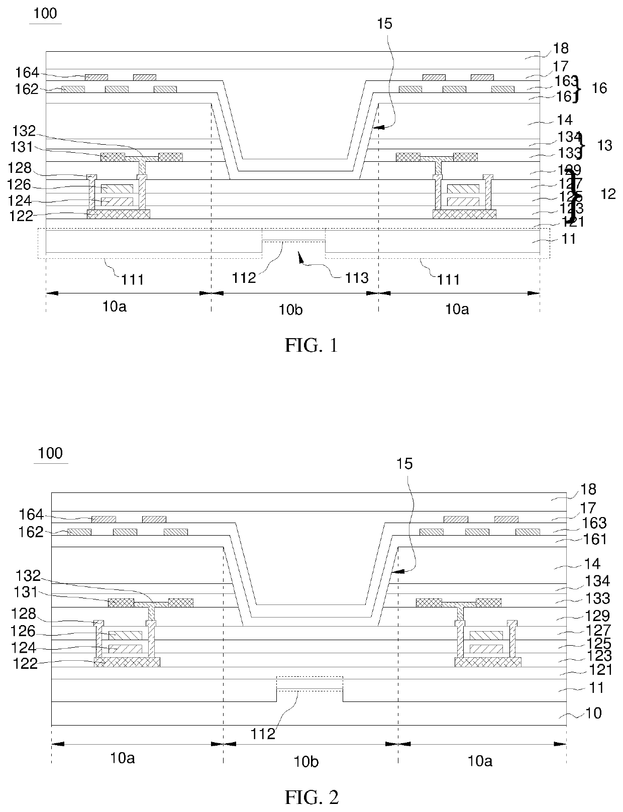
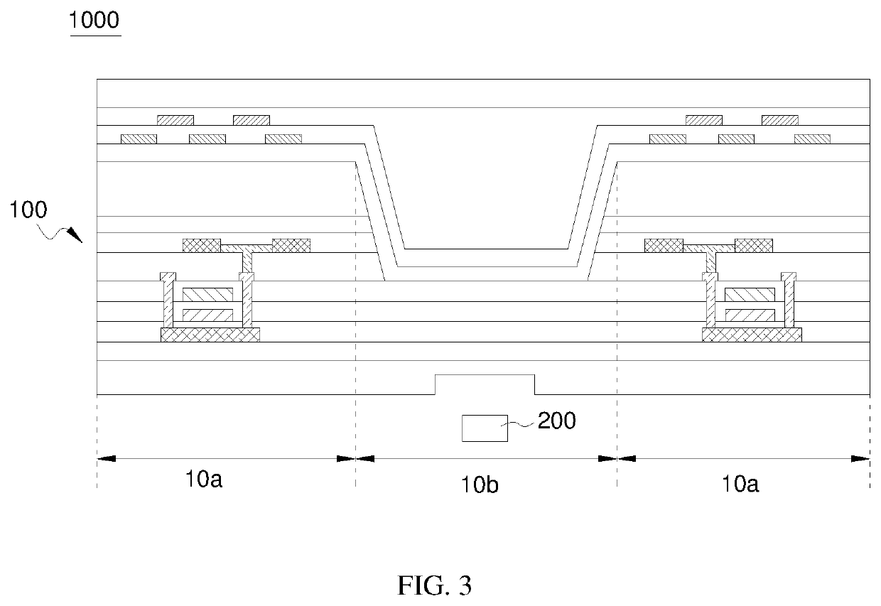
[0045]Please refer to FIG. 1. FIG. 1 shows a schematic structural diagram of an embodiment of an organic light emitting diode (OLED) display panel of the present invention. The OLED display panel 100 of an embodiment of the present invention includes a thin film transistor (TFT) structure layer 12, a light emitting functional layer 13, and an encapsulation layer 14 which are sequentially disposed on the substrate 11.

[0046]The OLED display panel 100 includes a light transmission area 10b and a display area 10a surrounding a periphery of the light transmission area 10b.

[0047]A concave groove 15 is disposed in the OLED display panel 100 corresponding to the light transmiss...


PUM


Abstract

The present invention provides an organic light-emitting diode (OLED) display panel and an OLED display device. The OLED display panel comprises a light transmission area and a display area surrounding a periphery of the light transmission area; a concave groove is disposed in the OLED display panel corresponding to the light transmission area, and the concave groove penetrates through at least an encapsulation layer, a light emitting function layer and a part of a thin film transistor (TFT) structure layer; and at least a part of a touch function layer extends from the display area toward the concave groove and covers the concave groove.

Description

BACKGROUND OF INVENTIONField of Invention[0001]The present invention relates to a display technology, and in particular, to an organic light emitting diode (OLED) display panel and an OLED display device.Description of Prior Art[0002]With gradual maturity of organic light emitting diode (OLED) technology, higher and higher requirements have been put forward on reliability of OLEDs, such as narrow bezel technologies, panel manufacturers realize OLED displays with bezel sizes of less than 2 mm through chip on film (COF) and / or chip on plastic (COP) technologies, resulting in a higher screen ratio when a camera is placed in a light emitting area of the OLED.[0003]In existing display panels, a built-in camera is generally set in a lower part of a display area, and a place for setting the camera is provided by cutting through the entire device by a laser from top to bottom or from bottom to top after completing the whole OLED process to form a through hole, and the camera is disposed in ...

Claims


Application Information

Patent Timeline
IPC IPC(8): H01L27/32H01L51/52
CPCH01L27/3258H01L27/323H01L51/5237H10K59/00H10K59/126H10K59/1213Y02E10/549H10K59/40H10K77/10H10K2102/351H10K59/124H10K50/84
Inventor JIN, JIANGJIANG
Owner WUHAN CHINA STAR OPTOELECTRONICS SEMICON DISPLAY TECH CO LTD
Why Eureka
Try Eureka