Method for producing a nanocrystalline, gas-sensitive layer structure
- Summary
- Abstract
- Description
- Claims
- Application Information
AI Technical Summary
Benefits of technology
Problems solved by technology
Method used
Image

Examples
Embodiment Construction
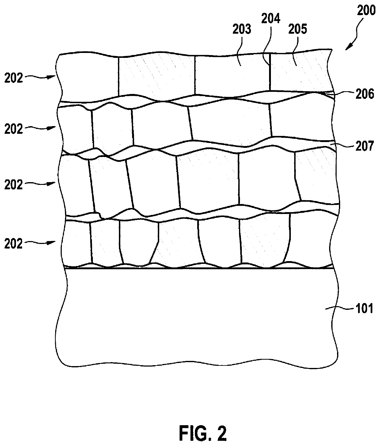
[0025]In the figures, identical reference symbols denote identical or functionally equivalent elements.
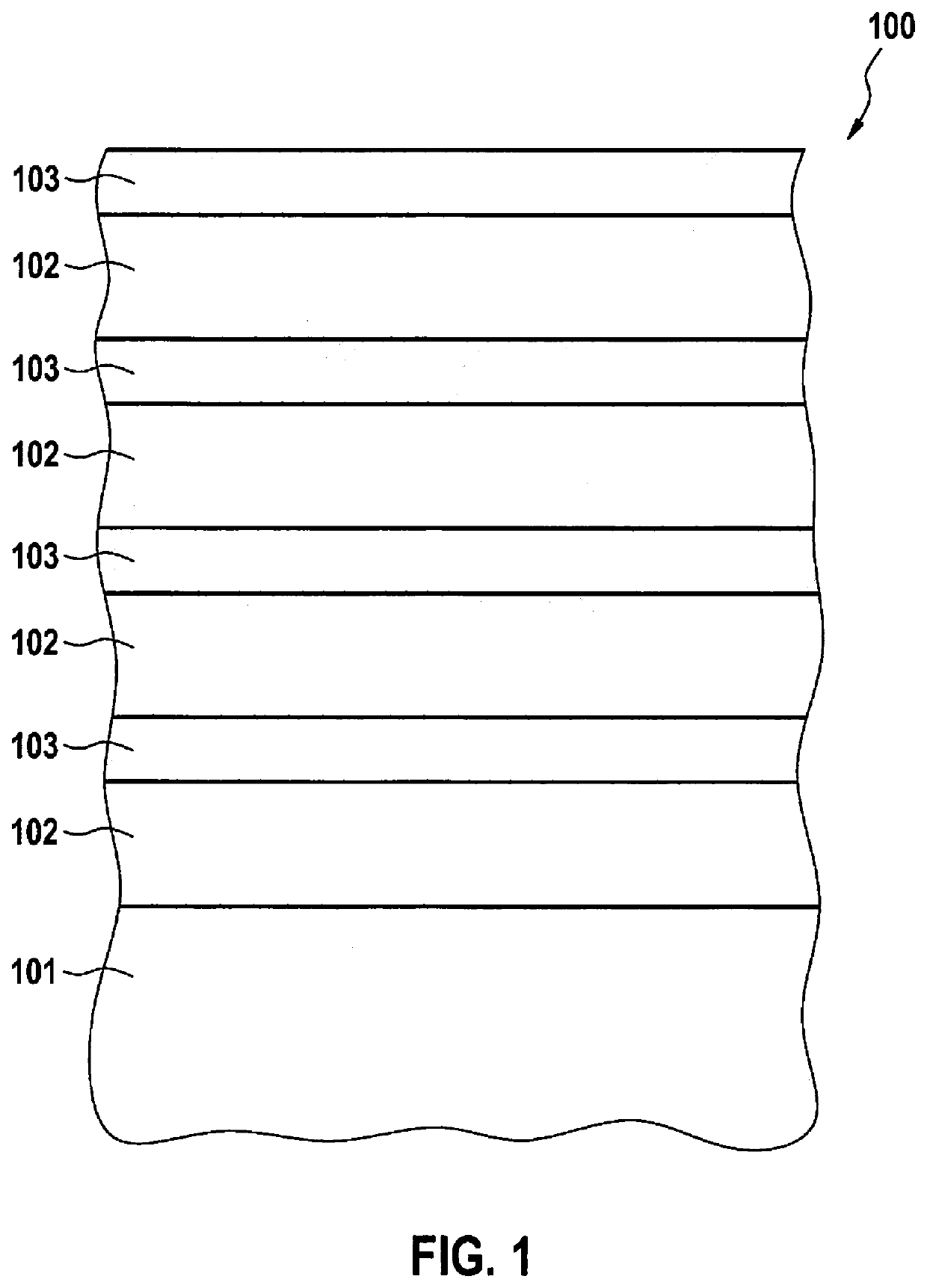
[0026]FIG. 1 is a schematic representation for explaining a layer structure according to a specific embodiment of the present invention prior to the tempering step, in a cross-sectional view.
[0027]FIG. 1 shows the case of an amorphous deposition of base material and doping material; while other morphologies are also possible, for example a base material that is already present after the deposition in partially crystalline form, the doping material already being able to penetrate along the grain boundaries during the deposition, but above all during the annealing step.
[0028]In FIG. 1, reference numeral 101 indicates an insulating layer (substrate), 102 indicates the base layers made of base material, 103 indicates a doping layer made of doping material and 100 indicates the entire layer structure following the deposition for example by sputtering or ALD processes prior to the temper...
PUM
| Property | Measurement | Unit |
|---|---|---|
| Temperature | aaaaa | aaaaa |
| Fraction | aaaaa | aaaaa |
| Thickness | aaaaa | aaaaa |
Abstract
Description
Claims
Application Information