A method for making external electrodes of electronic components

A technology for electronic components and external electrodes, applied in the field of external electrodes for making electronic components, can solve the problems of environmental pollution, dissatisfaction, time-consuming and material costs, etc., and achieve simple process maintenance, easy operation, and improved efficiency Effect

Active Publication Date: 2018-01-12
SHENZHEN SUNLORD ELECTRONICS
View PDF4 Cites 0 Cited by
  • Summary
  • Abstract
  • Description
  • Claims
  • Application Information

AI Technical Summary

Problems solved by technology

[0006] 1. By increasing the thixotropic index and viscosity of the slurry and adjusting the coating parameters, it takes a lot of time and material costs, not only the effect is not significant but also the consistency and reproducibility are poor;
[0007] 2. Hydrophobic modification treatment is carried out on the surface of multi-terminal chip components through hydrophobic liquid, so that the hydrophobic film layer formed on the surface of multi-terminal chip components has hydrophobic characteristics, and the degree of wetting, diffusion and sag of electrode slurry on the product surface is reduced , to improve the external electrode fish maw and burr-like defects, but its hydrophobic liquid is volatile at room temperature and produces irritating odors, which pollutes the working environment, and the hydrophobic treatment does not meet the metric size of 1608 or less

Method used


Image

  • A method for making external electrodes of electronic components
  • A method for making external electrodes of electronic components
  • A method for making external electrodes of electronic components

Examples


example 1

[0048] A method for plasma treatment of the surface of a multi-terminal component, comprising the following steps:

[0049] Step 1: Prefabricated target

[0050] The target is made of iron material into a rectangular box shape, the width and height of the box are 40cm, and the length of the box is made or segmented according to needs;

[0051] Step 2: Assembly

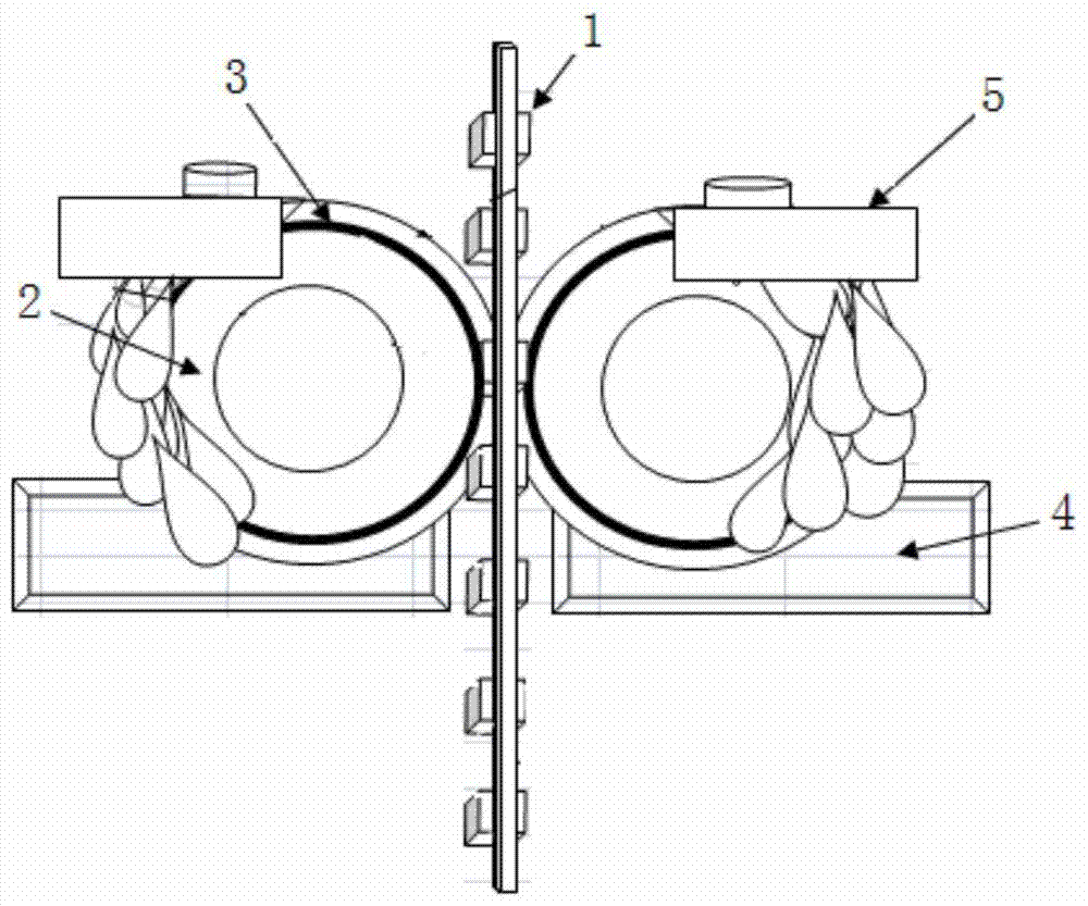
[0052] Place the multi-terminal chip components on the upper surface of the conveyor belt and pass through the middle of the target without contacting the target. The conveyor belt shaft is located at both ends of the target, and the target is placed in a vacuum chamber. The target, multi-terminal chip components and The conveyor belts are all insulated from the vacuum chamber;

[0053] Step 3: Load the monomer, ventilate, and power on

[0054] Load monomer HMDSO (hexamethyldisiloxane), feed argon as the carrier, set the target to negative potential, voltage -2600V; adjust the transmission shaft to keep the conveyor...

example 2

[0058] A method for plasma treatment of the surface of a multi-terminal component, comprising the following steps:

[0059] Step 1: Prefabricated target

[0060] The target is made of copper material into a rectangular box shape, the width and height of the box are 10cm, and the length of the box is made or segmented according to needs;

[0061] Step 2: Assembly

[0062] Place the multi-terminal chip components on the upper surface of the conveyor belt and pass through the middle of the target without contacting the target. The conveyor belt shaft is located at both ends of the target, and the target is placed in a vacuum chamber. The target, multi-terminal chip components and The conveyor belts are all insulated from the vacuum chamber;

[0063] Step 3: Load the monomer, ventilate, and power on

[0064] Load monomer HMDSO (hexamethyldisiloxane), feed argon as the carrier, set the target to negative potential, voltage -1000V; adjust the transmission shaft to keep the convey...

example 3

[0068] A method for plasma treatment of the surface of a multi-terminal component, comprising the following steps:

[0069] Step 1: Prefabricated target

[0070] The target is made of iron material into a rectangular box shape, the width and height of the box are 25cm, and the length of the box is made or segmented according to needs;

[0071] Step 2: Assembly

[0072] Place the multi-terminal chip components on the upper surface of the conveyor belt and pass through the middle of the target without contacting the target. The conveyor belt shaft is located at both ends of the target, and the target is placed in a vacuum chamber. The target, multi-terminal chip components and The conveyor belts are all insulated from the vacuum chamber;

[0073] Step 3: Load the monomer, ventilate, and power on

[0074] Load monomer HMDSO (hexamethyldisiloxane), feed argon as the carrier, set the target to negative potential, voltage -1800V; adjust the transmission shaft to keep the conveyor...


PUM


Abstract

The invention discloses a method for manufacturing an external electrode of an electronic component, comprising steps of performing plasma modification processing on the surface of an electronic element before the electronic member is coated by the external electrode, depositing on the surface of the electronic element to generate a uniform SiOx film layer, enabling the surface of the electronic element to obtain a certain draining performance on the surface, wherein the electronic element is particularly a multi-terminal sheet type element, and coating electrode slurry on the electronic element to form an external electrode. The invention also discloses a method for processing the surface of the electronic device, which enables the external electrode to be straight, smooth, non-fish-belly and non-burr.

Description

technical field [0001] The invention relates to a method for making external electrodes of electronic components. Background technique [0002] In recent years, with the application and continuous improvement of microelectronic circuit surface mount technology (SMT), lightness, thinness, shortness, and smallness have become important symbols for measuring electronic products. To miniaturize electronic equipment, we must first consider the electronic Miniaturization of components. After the miniaturization of electronic components, the precision and appearance requirements of the external electrodes of the products have also raised new heights. After the size of components is miniaturized, the size and spacing of terminal electrodes are getting smaller and smaller, especially for multi-terminal chip components such as filters, magnetic bead rows, and pressure-sensitive rows. Multiple electrodes are required on one terminal, such as external electrodes The accuracy and strai...

Claims


Application Information

Patent Timeline
Patent Type & Authority Patents(China)
IPC IPC(8): H01L21/60
CPCH01L24/85
Inventor 杨日章王清华许光
Owner SHENZHEN SUNLORD ELECTRONICS
Why Eureka
Try Eureka