Display device

a technology of display panel and display panel, which is applied in the direction of solid-state devices, basic electric elements, instruments, etc., can solve the problems of deterioration of the function achieve the effect of improving the optical sensing of the optical device, increasing the area of the transmission area, and increasing the amount of light incident on the optical device arranged on the back surface of the second display area of the display panel through the transmission area

Pending Publication Date: 2021-12-09
SAMSUNG DISPLAY CO LTD
View PDF7 Cites 2 Cited by
  • Summary
  • Abstract
  • Description
  • Claims
  • Application Information

AI Technical Summary

Benefits of technology

[0012]According to the aforementioned and other example embodiments of the present disclosure, a number of light emitting elements of the pixel in the second display area may be greater than a number of light emitting elements of the pixel in the first display area. In this case, a maximum luminance of the pixels in the second display area may be higher than a maximum luminance of the pixels in the first display area. Accordingly, a difference between the maximum luminance of the first display area and the maximum luminance of the second display area due to the transmission area can be minimized or reduced.
[0013]According to the aforementioned and other example embodiments of the present disclosure, when the area of the pixel in the second display area is reduced, the area of the transmission area may be increased. Therefore, the amount of light incident on the optical devices arranged on the back surface of the second display area of the display panel through the transmission areas can be increased. Thus, optical sensing of the optical devices may be improved.
[0014]According to the aforementioned and other example embodiments of the present disclosure, when the first alignment electrode and the second alignment electrode are disposed on a same layer as the sensing electrodes and the driving electrodes and are made of a same material as the sensing electrodes and the driving electrodes, the first alignment electrode, the second alignment electrode, the sensing electrodes, and the driving electrodes may be formed by one mask process. Therefore, any one of the mask process for forming the first alignment electrode and the second alignment electrode and the mask process for forming the sensing electrodes and the driving electrodes can be omitted, thereby reducing a manufacturing cost.
[0015]According to the aforementioned and other example embodiments of the present disclosure, when the sensor electrode is disposed on a same layer as the second contact electrode and is made of a same material as the second contact electrode, the sensor electrode and the second contact electrode can be formed by one mask process. Therefore, any one of the mask process for forming the sensor electrode and the mask process for forming the second contact electrode can be omitted, thereby reducing a manufacturing cost.

Problems solved by technology

Thus, the function of the optical device may be deteriorated.

Method used


Image

  • Display device
  • Display device
  • Display device

Examples


Embodiment Construction

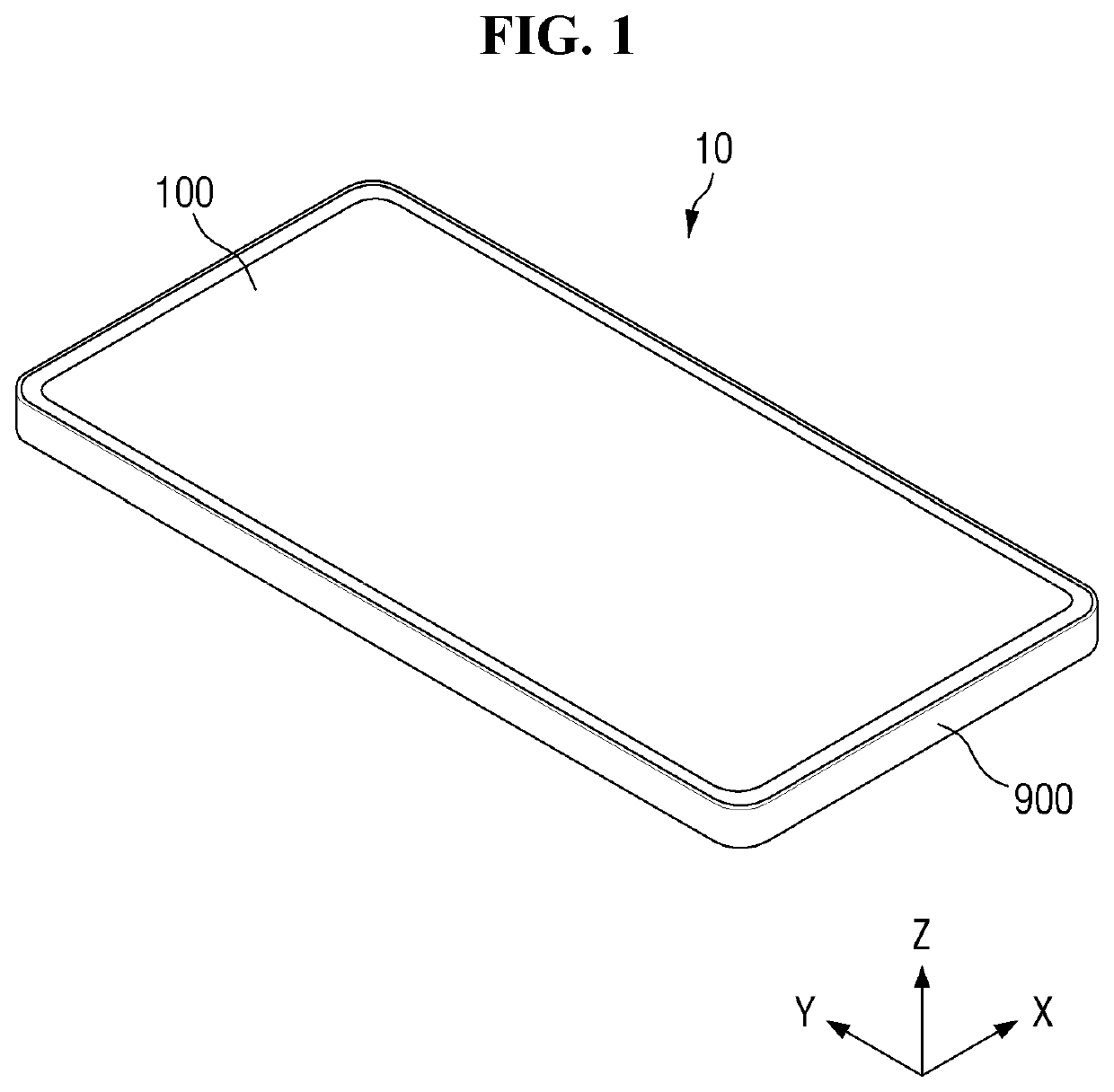
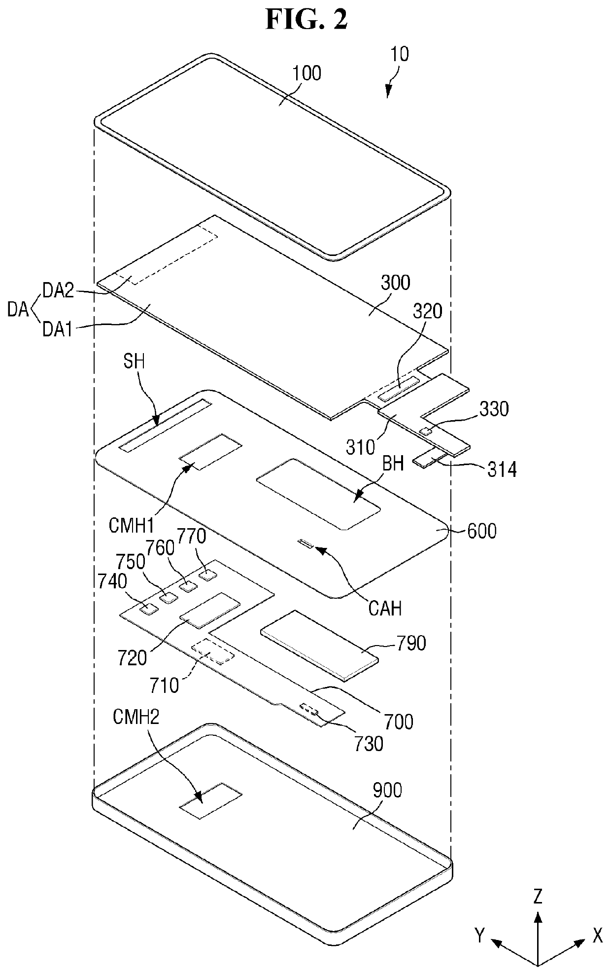
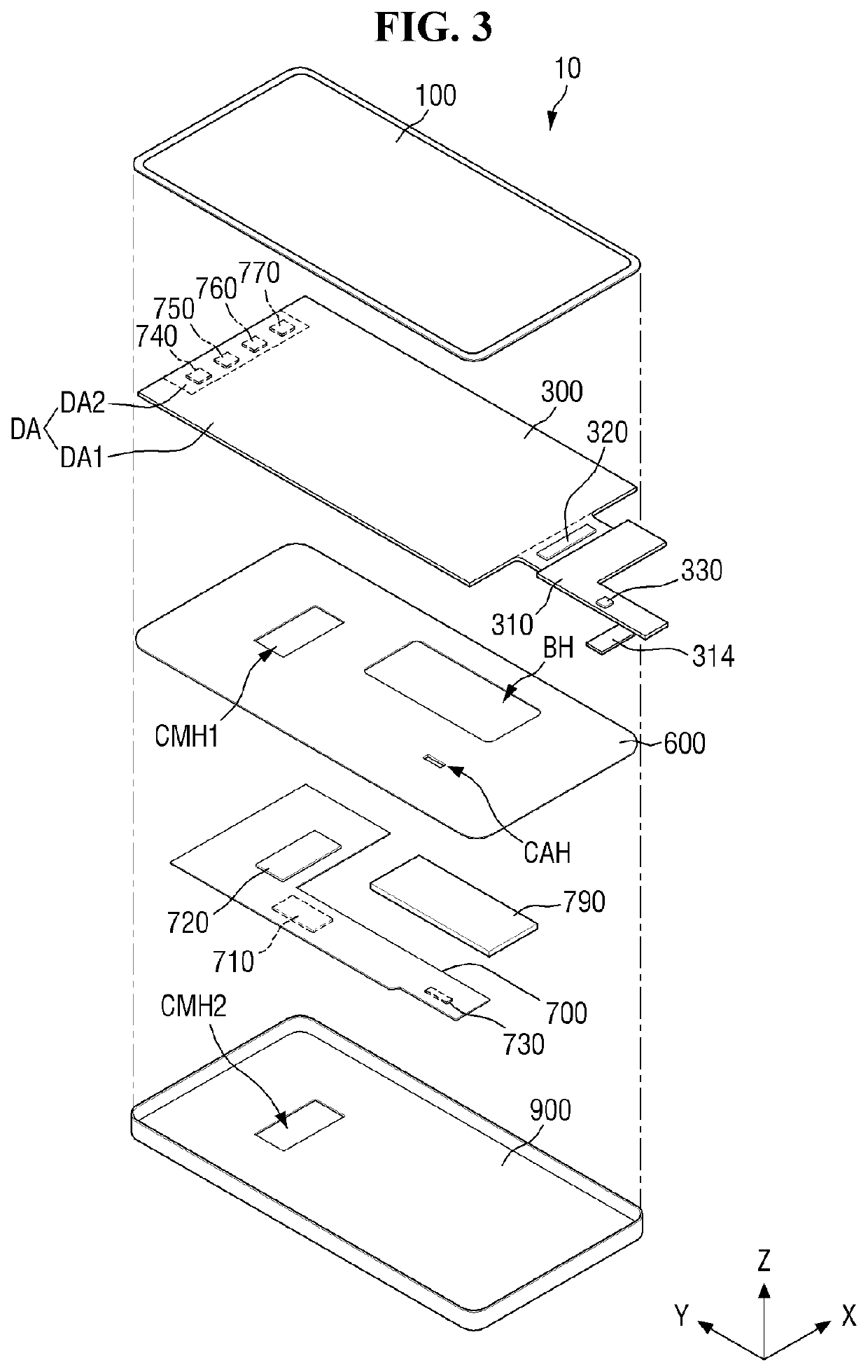
[0039]The present disclosure will now be described more fully herein with reference to the accompanying drawings, in which some example embodiments of the disclosure are shown. This disclosure may, however, be embodied in different forms and should not be construed as being limited to the embodiments set forth herein. Rather, these embodiments are provided so that this disclosure will be thorough and complete, and will fully convey the scope of the disclosure to those skilled in the art. The same reference numbers indicate the same or like components throughout the specification. In the attached figures, the thicknesses of layers and regions may be exaggerated for clarity.

[0040]Herein, the use of the term “may,” when describing embodiments of the present disclosure, refers to “one or more embodiments of the present disclosure.” As used herein, the term “and / or” includes any and all combinations of one or more of the associated listed items. As used herein, the singular forms “a,”“an...


PUM

PropertyMeasurementUnit
thicknessaaaaaaaaaa
area DAaaaaaaaaaa
lengthaaaaaaaaaa

Abstract

A display device includes: a display panel including a first display area including first sub-pixels to display an image, and a second display area including second sub-pixels and a transmission area adjacent to the second sub-pixels; and an optical device overlapping the second display area of the display panel and configured to detect light incident through the transmission area. Each of the second sub-pixels includes: a first contact electrode; a second contact electrode located apart from the first contact electrode; and a light emitting element between the first contact electrode and the second contact electrode.

Description

CROSS-REFERENCE TO RELATED APPLICATION[0001]This application claims priority to and the benefit of Korean Patent Application No. 10-2020-0069513, filed on Jun. 9, 2020 in the Korean Intellectual Property Office (KIPO), the entire content of which is incorporated by reference herein.BACKGROUND1. Field[0002]Aspects of embodiments of the present invention relate to a display device.2. Description of the Related Art[0003]With the development of information society, requirements for display devices for displaying images have increased in various forms. For example, display devices are applied to various electronic appliances, such as smartphones, digital cameras, notebook computers, navigators, and smart televisions.[0004]A display device may include a display panel including a plurality of pixels connected to scan lines, data lines, and power lines to display an image. Further, the display device may include various optical devices, such as an image sensor for photographing an image on ...

Claims


Application Information

Patent Timeline
Patent Type & Authority Applications(United States)
IPC IPC(8): H01L25/16H01L27/32H01L25/18G06F3/044G06F3/041
CPCH01L25/167H01L27/3248H01L25/18H01L33/62G06F3/044G06F3/0412H01L27/323H01L25/0753G06F3/0446H10K59/352H10K59/65H10K59/131H01L23/38H01L23/48H10K59/40H10K59/123
Inventor BOK, SEUNG LYONGRYU, AN NAKWAG, JIN OH
Owner SAMSUNG DISPLAY CO LTD
Why Eureka
Try Eureka