Supercharge Your Innovation With Domain-Expert AI Agents!

Cmp polishing pad with uniform window

a technology of polishing pads and windows, applied in the field of polishing pads, can solve the problems of non-uniform or non-planar and achieve the effect of avoiding the formation of a splinter or a splinter in the topography of the wafer

Active Publication Date: 2021-12-30
ROHM & HAAS ELECTRONICS MATERIALS CMP HLDG INC
View PDF0 Cites 1 Cited by
  • Summary
  • Abstract
  • Description
  • Claims
  • Application Information

AI Technical Summary

Benefits of technology

The patent is for a polishing pad used for chemical mechanical polishing of semiconductor, optical or magnetic substrates. The pad has a transparent window with a flexible top surface that is secured to the pad and has grooves for polishing. The window has a bending mechanism that allows it to bend around multiple axes, including non-parallel or center projecting elements. This mechanism reduces contact pressure with the substrate during polishing without compromising the effectiveness of the polishing process. The technical effect of this invention is to improve the polishing efficiency and quality of the polishing process while reducing the risk of damage to the substrate.

Problems solved by technology

As layers of materials are sequentially deposited and removed, the topography (i.e. uppermost surface) of the wafer becomes non-uniform or non-planar.

Method used


Image

  • Cmp polishing pad with uniform window
  • Cmp polishing pad with uniform window
  • Cmp polishing pad with uniform window

Examples


example 1

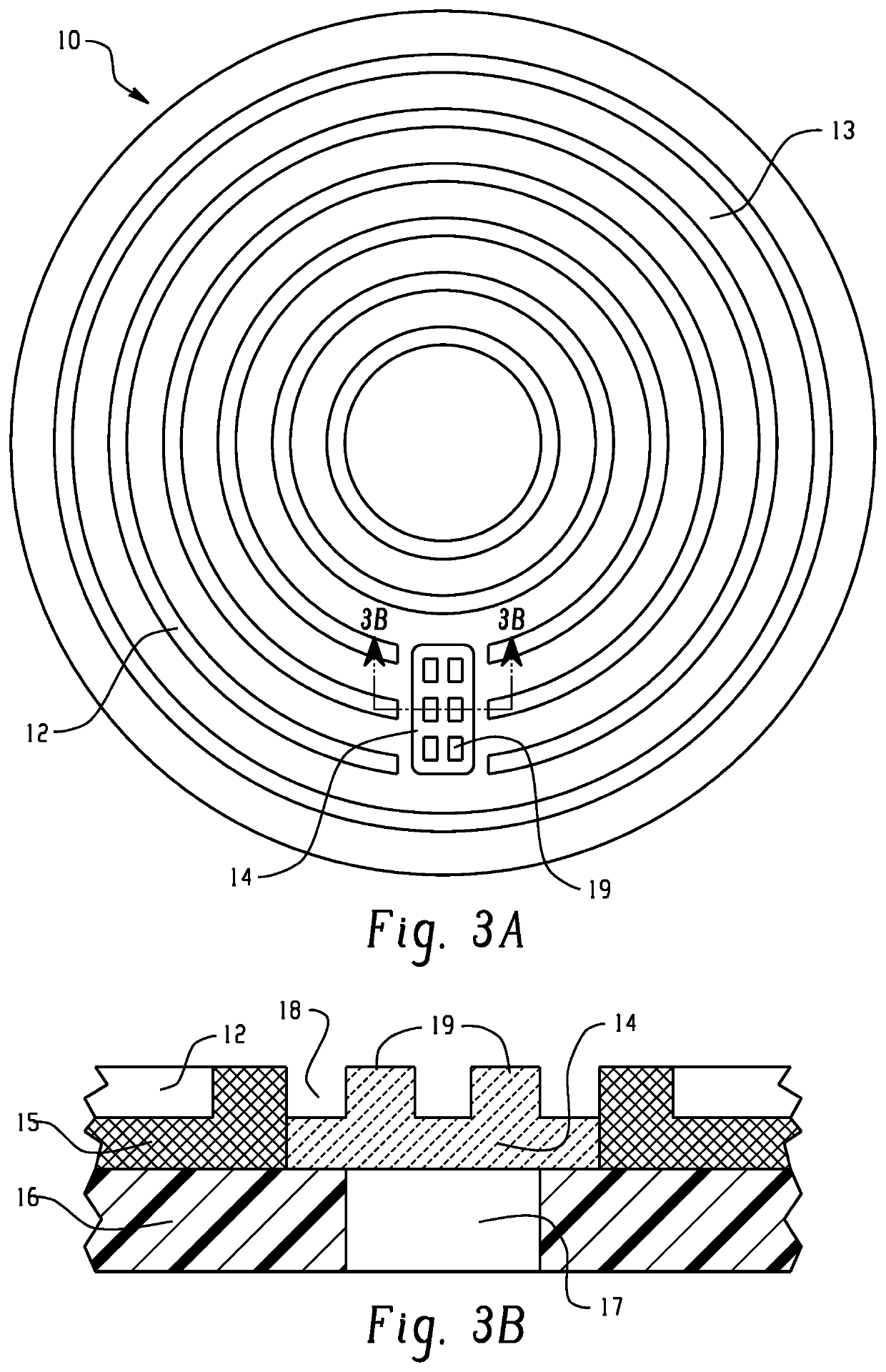
[0057]A polishing pad was prepared that incorporates a window of the design illustrated in Drawing 5. The window (301) was circular, with a diameter of 18 mm and a thickness of 2.032 mm. These dimensions are equivalent to those found in prior art window pads. Samples were made from several materials capable of transmitting UV / visible light in the wavelength range of 250-800 nm.

[0058]The recess design consists of a central raised region or element (303) of 6 mm in diameter that has no recesses, and an outer region of eight polygonal raised areas or elements (303′). The surface of all raised elements was coplanar with the polishing pad top surface, and the bottom of the window (301) is coplanar with the interface between the polishing portion (i.e. polishing layer) and lower layers (i.e. sublayer or base layer) of the polishing pad. Between central and polygon regions, there is a circular recessed area (302) of 1.524 mm width and 0.762 mm depth. Each polygon raised area (303′) was sep...


PUM

PropertyMeasurementUnit
Young's modulusaaaaaaaaaa
sizeaaaaaaaaaa

Abstract

A polishing pad useful in chemical mechanical polishing comprising a polishing portion having a top polishing surface and comprising a polishing material an opening through the polishing pad, and a transparent window within the opening in the polishing pad, the transparent window being secured to the polishing pad and being transparent to at least one of magnetic and optical signals, the transparent window having a thickness and a top surface having a plurality of elements separated by interconnected recesses to provide a pattern in the top surface that includes recesses for improved deflection into a cavity in the polishing pad during polishing.

Description

FIELD OF THE INVENTION[0001]The present invention relates generally to the field of polishing pads for chemical mechanical polishing. In particular, the present invention is directed to a chemical mechanical polishing pad having a polishing structure useful for chemical mechanical polishing of magnetic, optical and semiconductor substrates, including front end of line (FEOL) or back end of line (BEOL) processing of memory and logic integrated circuits.BACKGROUND[0002]In the fabrication of integrated circuits and other electronic devices, multiple layers of conducting, semiconducting and dielectric materials are deposited onto and partially or selectively removed from a surface of a semiconductor wafer. Thin layers of conducting, semiconducting and dielectric materials may be deposited using several deposition techniques. Common deposition techniques in modern wafer processing include physical vapor deposition (PVD), also known as sputtering, chemical vapor deposition (CVD), plasma-e...

Claims


Application Information

Patent Timeline
Patent Type & Authority Applications(United States)
IPC IPC(8): B24B37/20B24B37/04
CPCB24B37/205B24B37/042B24B37/20B24B37/26B24B37/24B24B37/013B24B37/10H01L21/67092
Inventor GUZMAN, MAURICIO E.VASQUEZ, NESTOR A.GADINSKI, MATTHEW R.MILLS, MICHAEL E.
Owner ROHM & HAAS ELECTRONICS MATERIALS CMP HLDG INC
Features
  • R&D
  • Intellectual Property
  • Life Sciences
  • Materials
  • Tech Scout
  • Unparalleled Data Quality
  • Higher Quality Content
  • 60% Fewer Hallucinations
Learn More